Part No:
5AGXBB1D4F35C4G
Category:
Programmable Logic ICs
Description:
The Arria® V device family consists of the most comprehensive offerings of mid-range FPGAs ranging from the lowest power for 6 gigabits per second (Gbps) and 10 Gbps applications, to the highest mid-range FPGA bandwidth 12.5 Gbps transceivers.
Stock Status:
Available for RFQ
Pricing:
Request Volume Pricing
Quote Response:
Within 24 Hours
Shipping:
In-stock parts ship in 1–2 business days
Specification
Operating Temperature Industrial
Operating Temperature Commercial
Package Type
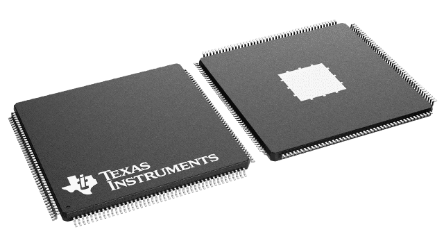
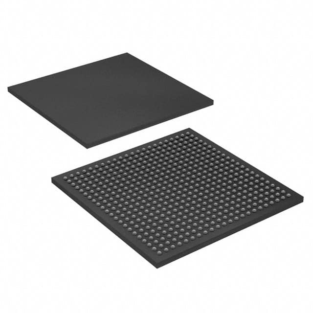
Thermal composite flip chip BGA
Products Detail
Arria V devices are ideal for power-sensitive wireless infrastructure equipment, 20G/40G bridging, switching, and packet processing applications, high-definition video processing and image manipulation, and intensive digital signal processing (DSP) applications. Key advantages include lowest static power in its class, improved logic integration and differentiation capabilities, increased bandwidth capacity, hard processor system with integrated ARM Cortex-A9 MPCore processor, and lowest system cost. The devices are built on TSMC's 28 nm process technology and include an abundance of hard intellectual property (IP) blocks, power-optimized MultiTrack routing and core architecture, and up to 50% lower power consumption than the previous generation. They feature 8-input adaptive logic module (ALM), up to 38.38 Mb of embedded memory, variable-precision DSP blocks, serial data rates up to 12.5 Gbps, hard memory controllers, and a dual-core ARM Cortex-A9 MPCore processor integrated with FPGA in a single SoC.
Key Features
- Technology: TSMC 28nm process (28LP for GX, GT, SX, ST; 28HP for GZ)
- Packaging: Thermal composite flip chip BGA, multiple device densities with identical package footprints, leaded and lead-free options
- FPGA fabric: Enhanced 8-input ALM with four registers, improved routing architecture
- Internal memory: M10K (with soft ECC for GX, GT, SX, ST), M20K (with hard ECC for GZ), MLAB (640-bit distributed LUTRAM)
- Variable-precision DSP: Native support for up to four signal processing precision levels, 64-bit accumulator, preadder/subtractor
- Memory controller: DDR3 and DDR2 (for GX, GT, SX, ST)
- Embedded transceiver I/O: Up to 6.5536 Gbps (GX, SX), 10.3125 Gbps (GT, ST), 12.5 Gbps (GZ)
- PCIe: Gen2 (x1, x2, x4) and Gen1 (x1, x2, x4, x8) hard IP, Gen3 (x1, x2, x4, x8) support for GZ
- Ethernet and other PCS: GbE, XAUI, CPRI, GPON, 10GbE (GZ), SRIO, Interlaken (GZ)
- Clock networks: Up to 650 MHz global clock, power-down capability
- Phase-locked loops (PLLs): High-resolution fractional PLLs, precision clock synthesis
- FPGA GPIOs: 1.6 Gbps LVDS, 800 MHz/1.6 Gbps external memory interface, 3.3V support
- External memory interface: Hard memory controller up to 1.066 Gbps, soft up to 1.6 Gbps
- Low-power high-speed serial interface: 600 Mbps to 12.5 Gbps, less than 105 mW per channel at 6 Gbps, less than 165 mW per channel at 10 Gbps, less than 170 mW per channel at 12.5 Gbps, transmit pre-emphasis and receiver equalization, dynamic partial reconfiguration
- HPS (for SX and ST): Dual-core ARM Cortex-A9 MPCore processor up to 1.05 GHz, interface peripherals (Ethernet, USB 2.0 OTG, QSPI, NAND, SD/MMC, UART, SPI, I2C, up to 85 HPS GPIO), system peripherals (timers, watchdog, DMA, configuration manager, clock and reset managers), on-chip RAM and boot ROM, HPS-FPGA bridges, FPGA-to-HPS SDRAM controller subsystem, ARM CoreSight JTAG debug
- Configuration: Tamper protection, AES design security, Configuration via Protocol (CvP), dynamic reconfiguration, active serial (AS) x1 and x4, passive serial (PS), JTAG, fast passive parallel (FPP) x8, x16, x32 (GZ), remote system upgrade.
Application scenarios
- power-sensitive wireless infrastructure equipment
- 20G/40G bridging
- switching
- and packet processing applications
- high-definition video processing and image manipulation
- intensive digital signal processing (DSP) applications
Documents