TMS320F28335PGFA MCU: Compare C2000 Migration Options
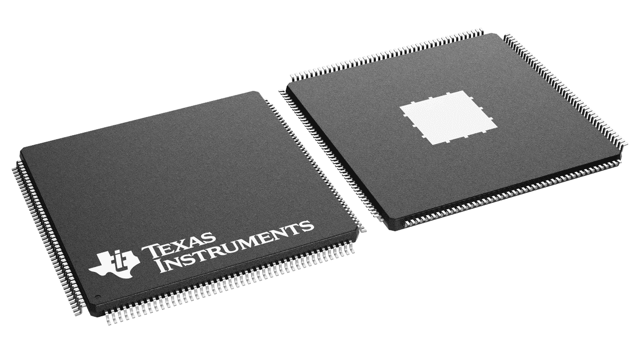
TMS320F28335PGFA is a Texas Instruments C2000 microcontroller with a 150 MHz C28x core, single-precision floating-point support and a 176-pin LQFP package. Its control application depends on more than processor speed. Comparing another C2000 device requires preserving the relationship between ADC sampling, PWM updates, memory access and fault handling, while checking the exact package, supply rails and software support.
Key Takeaways
- Choose the migration objective before choosing the processor. More processing headroom, fewer pins and preservation of an existing board lead to different shortlists.
- The F28335 baseline has 256K × 16 flash and 34K × 16 RAM: 512 KiB and 68 KiB when expressed as eight-bit octets. Physical banks and access permissions matter alongside totals.
- Two ADC sample-and-hold circuits share one converter. Simultaneous acquisition does not mean every channel has an independent conversion engine.
- F28377DPTPT, F28069PZT and F28035PAGT represent different redesign directions. F2812PGFA is a historical comparison point. None is declared a drop-in replacement here.
- A migration passes when the intended control behavior survives startup, normal operation, communications load and faults. A successful build is only an early checkpoint.
Define the Design That Must Survive Migration
A useful TMS320F28335PGFA migration review starts with the present design's obligations. Identify the signals it samples, the deadlines it meets, the outputs it must inhibit during a fault and the information it must retain through an update. Only then compare a prospective device with that baseline.
The distinction is practical. A product with spare processing time but too many external components may benefit from a different integration strategy. A product missing its control deadline needs evidence about execution and peripheral timing. A board maintained for service may place greater value on keeping the approved implementation unchanged. Those are separate engineering goals, even when all three begin with the same part-number search.
Table 1. Establish the exact source-device baseline.
| Item | TMS320F28335PGFA baseline | Boundary to preserve |
|---|---|---|
| Processor | One C28x core, up to 150 MHz, single-precision FPU | Clock frequency is not a complete application benchmark |
| Flash | 256K × 16; 512 KiB octet equivalent | Program/erase operation and sector allocation affect usable design space |
| RAM | 34K × 16; 68 KiB octet equivalent | Not every bank is DMA-accessible or identical for CPU instruction access |
| ADC | 12-bit, 16 inputs, two sample-and-hold circuits, one converter | Up to 12.5 MSPS under specified conditions is not a per-channel promise |
| Main PWM resources | Six ePWM modules providing 12 A/B outputs | Six eCAP blocks can also provide auxiliary PWM; these are different resources |
| Core supply at 150 MHz | 1.9 V nominal; 1.805–1.995 V recommended range | The lower-voltage, lower-frequency condition is not interchangeable |
| Exact package and grade | PGF 176-pin LQFP; A ambient range −40 to 85°C | Do not substitute the PTP thermal package or another temperature suffix |
Table 1: Source identity and operating boundaries | Source: TI SPRS439Q, pp. 1–2, 8–9, 34, 108, 114–115, 183 and exact ordering row p. 194 | Compiled by: icallin.com
Keep a copy of the existing linker map, compiler options, schematic revision and initialization sequence beside this table. They establish what the application actually uses. A family feature list cannot reveal whether a buffer occupies a particular RAM bank, an interrupt depends on a legacy vector, or a boot strap shares a signal needed elsewhere.
The most useful starting measurement would be the worst observed execution and acquisition timing under representative system load. This article does not report such a measurement. It proposes the evidence a migration project should collect and connects that evidence to manufacturer limits. That keeps a design review from confusing a plausible candidate with a demonstrated result.
Compare Five Exact C2000 Ordering Codes by Their Role
C2000 migration options should be divided by purpose before comparing headline numbers. The following exact ordering codes are present in icallin's current model pool. Their links identify products; their engineering roles come from the source datasheet and the manufacturer's exact ordering pages.
Table 2. A shortlist for different redesign objectives.
| Exact ordering code | Processor / maximum clock | Published flash | Exact package | Role in this comparison |
|---|---|---|---|---|
| TMS320F28335PGFA | Single C28x with FPU; 150 MHz | 512 KB | PGF, 176-pin LQFP | Existing-design baseline |
| TMS320F28377DPTPT | Two C28x cores with FPU; 200 MHz per core | 1024 KB | PTP, 176-pin HLQFP | More processing resources, subject to substantial integration work |
| TMS320F28069PZT | Single C28x with FPU; 90 MHz | 256 KB | PZ, 100-pin LQFP | Smaller-pin-count design if the application fits |
| TMS320F28035PAGT | C28x; 60 MHz; separate CLA resource | 128 KB | PAG, 64-pin TQFP | Reduced-resource design with a new allocation of functions |
| TMS320F2812PGFA | Fixed-point C28x; 150 MHz | 256 KB | PGF, 176-pin LQFP | Historical baseline, not a forward-upgrade recommendation |
Table 2: Genuine related models with distinct engineering roles; KB labels follow TI's product pages | Source: F28335 datasheet and TI exact F28377DPTPT, F28069PZT, F28035PAGT and F2812PGFA pages | Compiled by: icallin.com
Add Processing Resources Only When the Software Can Use Them
F28377DPTPT is the most obvious growth candidate within this selected set. Its two C28x cores and additional accelerator resources create options for partitioning work. They do not make an unchanged single-core application run at the sum of both clock frequencies. Define which work runs on each processor, what information crosses between them and how startup establishes ownership before using core count as a selection argument.
The physical change is equally important. TI identifies a 1.2 V core design for the F28377D family, whereas the source F28335 at 150 MHz uses the 1.9 V condition in Table 1. The exact target uses PTP HLQFP rather than the source PGF LQFP. Matching the number 176 does not validate the power tree, pad arrangement, thermal construction or pin assignments. These facts require a schematic and footprint review before a target board is released. TI F28377D exact product information.
Reduce the System Only After Removing Requirements
F28069PZT and F28035PAGT belong in a redesign discussion when the intended application can accept their smaller memory and pin allocations. They should not be described as universal upgrades from a 150 MHz, 512 KB source device. List the functions to retain, simplify or remove, and demonstrate that the resulting program and I/O allocation fit the exact target package.
The CLA deserves its own line in that allocation. A separate control accelerator is not interchangeable with a floating-point unit attached to the main CPU. Moving work to it introduces its own supported instruction, data access, triggering and integration questions. The F28035 entry therefore identifies the resource without implying that unchanged F28335 floating-point code can simply run on the main processor.
F2812PGFA supplies a useful historical check on assumptions: equal clock frequency and pin count can accompany less flash and a different control-peripheral architecture. TI identifies its Event Manager resources, whereas the F28335 design uses ePWM modules. Its place in the table is to expose that distinction, not to recommend moving a product backward or to predict future availability. TI F2812 exact product information.
Treat Memory as an Access Map, Not Just a Capacity Number
The F28335 memory terminology can cause an early comparison error. Its datasheet specifies 256K × 16 flash and 34K × 16 RAM. Multiplying each 16-bit word by two eight-bit octets gives the capacity equivalents used here. This is a storage comparison; it does not redefine the C28x compiler's addressing units or the meaning of a C object in a particular toolchain.
The RAM total contains two smaller M blocks and eight L blocks. A second address mapping of a physical bank does not add another bank. Counting both mappings would overstate the available memory before the migration even begins.
Table 3. Physical RAM and access distinctions on the source device.
| Physical bank group | Capacity in 16-bit words | Eight-bit-octet equivalent | Source access distinction |
|---|---|---|---|
| M0 | 1K × 16 | 2 KiB | CPU RAM; not a DMA destination in the listed DMA map |
| M1 | 1K × 16 | 2 KiB | CPU RAM; not a DMA destination in the listed DMA map |
| L0–L3 | Four banks, each 4K × 16 | 32 KiB total | DMA has no access; dual mapping does not duplicate physical storage |
| L4–L7 | Four banks, each 4K × 16 | 32 KiB total | DMA-accessible; CPU data and program access have different listed waits |
| Physical total | 34K × 16 | 68 KiB | Capacity total does not establish simultaneous-access performance |
Table 3: F28335 physical RAM allocation and access boundaries | Source: TI SPRS439Q, pp. 108, 115, 160 and 165 | Compiled by: icallin.com

The immediate implication is that a DMA buffer cannot be placed wherever the linker finds spare space. A buffer that fits in total RAM may still occupy an inaccessible bank. Preserve the required access relationship explicitly in the linker configuration and inspect the resulting map after changes to libraries, optimization settings or feature selection.
Zero memory wait states do not mean zero transfer cost. The source datasheet lists a basic DMA throughput of four cycles per word, with additional qualifications for particular accesses and conflicts. Its RAM timing table also distinguishes L4–L7 CPU data access from program access. Treating every bank as identical would hide both placement and timing problems. TI SPRS439Q, pp. 115–116 and 165.
An illustrative buffer calculation makes the allocation visible. Assume eight channels, 256 retained sample sets and one 16-bit storage word per channel. That requires 2,048 words, or 4 KiB in octet terms. Two such buffers require 8 KiB, equal to one L-bank's nominal capacity. This is arithmetic, not a proposed linker layout: alignment, metadata, other allocations and concurrent access can require a different placement.
Recheck Flash Timing Before Comparing Execution Speed
A clock-frequency comparison omits the memory conditions under which instructions are fetched. The source datasheet gives minimum flash and OTP wait-state settings at listed clock frequencies. They are configuration constraints, not measured loop execution times.
Table 4. Selected source-device clock points and minimum wait states.
| SYSCLKOUT | Minimum flash page wait states | Minimum flash random wait states | Minimum OTP wait states |
|---|---|---|---|
| 4 MHz | 1 | 1 | 1 |
| 15 MHz | 1 | 1 | 1 |
| 25 MHz | 1 | 1 | 1 |
| 30 MHz | 1 | 1 | 1 |
| 50 MHz | 1 | 1 | 2 |
| 75 MHz | 2 | 2 | 4 |
| 100 MHz | 3 | 3 | 5 |
| 120 MHz | 4 | 4 | 7 |
| 150 MHz | 5 | 5 | 8 |
Table 4: Published minimum flash and OTP wait states at listed source clock frequencies | Source: TI SPRS439Q, Table 7-4, p. 99 | Compiled by: icallin.com

A meaningful execution comparison should therefore retain the original code-placement record. Identify which time-critical routines execute from RAM, which tables remain in flash, which compiler options were used and whether a timing result came from a debug or production build. Then repeat the intended test on the target implementation under comparable application load. No frequency ratio can substitute for that record.
Firmware update behavior needs separate attention. The source cannot execute code from flash or OTP while flash is being programmed or erased, even if another flash sector is involved. The datasheet describes the associated RAM execution requirement. A migration that changes the updater, bootloader or memory partition must revisit this path as well as the normal control loop. TI SPRS439Q, p. 108.
Preserve a recovery scenario in the qualification plan. Record what the product should do after an interrupted update and which image or communication path restores operation. This is an application requirement, not a claim that the listed MCUs provide a particular recovery architecture automatically. It helps prevent an otherwise successful peripheral port from shipping with an unexamined maintenance path.
Preserve the ADC Measurement, Not Only the Channel Count
C2000 ADC migration needs to preserve when a signal was acquired, how it was converted and how software interprets the result. The F28335 has two sample-and-hold circuits and two sequencers around one conversion engine. Its simultaneous mode captures an A/B pair together, then makes the conversion results available in sequence. It does not turn sixteen inputs into sixteen simultaneous converters.
Table 5. Source ADC details that can change the meaning of a ported measurement.
| Source feature | Datasheet fact | Migration question |
|---|---|---|
| Analog input span | 0–3 V relative to ADCLO | Does the target input range preserve the existing signal-conditioning design? |
| Resolution | 12 bits | Are scaling, saturation and representation handled consistently? |
| Conversion clock | Up to 25 MHz under the specified source conditions | Was a CPU clock change incorrectly treated as an ADC clock setting? |
| Simultaneous pairing | A0/B0 through A7/B7 | Does the required pair retain the intended acquisition relationship? |
| Result access in peripheral frame 2 | Left-justified result; two CPU wait states | Does copied code shift and mask the correct representation? |
| Result access in peripheral frame 0 | Right-justified result; one CPU wait state, zero DMA memory wait states | Does the selected access path agree with the buffer format and DMA setup? |
| Calibration | Factory values must be loaded through the supported initialization path | Does debug startup or an ADC module reset omit required calibration? |
Table 5: F28335 ADC acquisition, result representation and initialization boundaries | Source: TI SPRS439Q, pp. 47, 100–104, 127 and 132–133 | Compiled by: icallin.com
Keep Acquisition Time Separate from Result Availability
At the source's 25 MHz ADC clock, one ADC clock period is 40 ns. The published acquisition-window relationship is one plus the selected acquisition setting in clock periods. A shortest acquisition window is therefore not the complete delay from trigger to usable control information. Conversion pipeline timing, the selected operating mode, result transfer and software scheduling add their own relationships.
This distinction matters when evaluating a sensor buffer or changing the trigger sequence. The input circuit must settle during acquisition, while the control task must receive the appropriate completed result before its deadline. Record those as separate requirements. Increasing a conversion clock without checking either requirement can preserve a plausible sample count while degrading the measurement or using data from the wrong event.
The source's analog specifications also qualify linearity by ADC clock range. A headline maximum throughput is therefore not the only meaningful acquisition setting. Select the operating point for the actual accuracy and timing budget, then compare a target at its own documented conditions. The target datasheets have not been used here to construct a numerical ADC performance ranking.
Make Result Representation and Calibration Explicit
A raw register value is not yet an engineering measurement. A left-justified 12-bit result and a right-justified result require different interpretation even though both originate from the same converter. A migration review should trace the selected register path through DMA or CPU transfer, buffer storage, scaling, filtering and the final control variable.
A useful proposed test supplies known input conditions and inspects values at each stage. This can expose a shifted result, swapped channel or stale buffer that a final output check might conceal. Keep these tests within the permitted analog range and the board's own operating requirements; the article provides no register-writing recipe or claim of completed measurements.
Calibration must also survive the execution path. TI specifically addresses debugging that bypasses the boot ROM and the need to initialize the ADC calibration registers appropriately; an ADC module reset requires the calibration process again. A design that works only under one debugger launch sequence has not established reproducible product startup. TI SPRS439Q, pp. 132–133.
Preserve PWM and Fault Behavior Across Startup and Shutdown
C2000 PWM migration is best specified as observable behavior. Record the required output frequency, relationship between channels, update event, dead time where used and response to each fault input. A list of peripheral register names is less durable because a different device can organize similar functions differently.
The source contains six ePWM modules, each with A/B outputs. Its eCAP modules can provide additional PWM functions, but those outputs should not be counted as interchangeable members of the main ePWM set. High-resolution capability also has a defined placement: the source describes HRPWM on the A path. A requirement that assumes the same capability on every output needs correction before target selection. TI SPRS439Q, pp. 114, 119 and 122.
Preserve safe output behavior through initialization, not just after initialization. The source datasheet distinguishes reset pull-up behavior between GPIO groups, and its low-power description says PWM states are retained as they were left. Entering a low-power mode is therefore not, by itself, a definition of the required inactive power-stage state. The application must specify and validate its intended sequence. TI SPRS439Q, pp. 22 and 180.
Pin multiplexing belongs in the same review. On the source device, GPIO functions can share PWM, CAN and ADC trigger-output roles. A design cannot assume that every family feature is simultaneously available on the chosen pins. Draw the complete pin allocation with boot, programming and fault signals included before accepting a smaller package or a new routing plan.
Fault-response numbers need their original endpoints. The source's specified trip-input-to-output timing is not a guarantee for the whole chain from sensor fault through external circuitry to power-stage shutdown. A proposed acceptance test should identify where the event is applied, where the response is observed and which delays belong outside the MCU. That produces a useful comparison without overstating a silicon timing number.
Rebuild the Software Contract and the Qualification Record
The software review should cover the toolchain, startup files, linker configuration, interrupt routing, peripheral access width and library dependencies. Keep the mathematical control algorithm distinguishable from the hardware-facing code so that a port does not hide changed assumptions inside an apparently familiar function name.
For this source family, even access width deserves attention: the datasheet gives different restrictions for eCAN control registers and other peripheral areas. A generic memory-copy approach is not evidence of a valid peripheral port. Likewise, the presence of a C28x core does not establish that old headers, interrupt numbers or linker files are appropriate for another device. TI SPRS439Q, pp. 140 and 165–171.
TI's current software guide identifies C2000Ware as the successor to controlSUITE and distinguishes migrated device-support components from older application content that remains in the legacy package. Use the documented support for the chosen device and record the actual versions used. Do not interpret an old project opening successfully in an IDE as a complete migration or assume every legacy example receives continuing updates. TI C2000 software guide: legacy components.
The release record should connect each requirement with evidence. For acquisition, preserve channel identity, timing and scaling. For outputs, preserve update timing and fault behavior. For communications, verify behavior while control work is active. For memory, retain map and access checks. For startup and maintenance, exercise the intended boot and update paths. These are proposed qualification activities, not test results reported by icallin.
This sequence makes a comparison more useful to sourcing as well. A candidate can be marked as under evaluation, approved for a particular board revision or rejected for a stated reason. The Texas Instruments product collection can help identify exact commercial entries, while the engineering record determines whether any entry is acceptable for the build.
Frequently Asked Questions
Q1: Is F28377DPTPT a drop-in replacement for TMS320F28335PGFA?
No drop-in relationship is established here. The exact devices have different core-supply requirements and package designations, and their processing and peripheral resources require a new integration review. The shared 176-pin count does not approve the schematic, footprint or firmware. Treat F28377DPTPT as a redesign candidate until those checks and application qualification are complete.
Q2: Does 34K × 16 RAM mean only 34 KB of storage?
It describes 34K sixteen-bit words, equivalent to 68 KiB when counted as eight-bit octets. That conversion does not make all memory interchangeable: the source DMA can access L4–L7, while L0–L3 are outside its access map. Retain both the capacity units and the physical bank allocation when comparing a linker map with a datasheet.
Q3: Can F28335 sample all sixteen ADC inputs simultaneously?
No. It has two sample-and-hold circuits sharing one converter. Simultaneous mode supports the defined A/B channel pairs, and their conversion results become available sequentially. A requirement for several signals to be acquired together must be mapped to the exact source and target acquisition architectures, not inferred from the total number of input pins.
Q4: Is F28069PZT automatically a better replacement because it has a CLA?
No. It is a different allocation of resources, with a 90 MHz main CPU, 256 KB published flash and a 100-pin package in the selected ordering code. A separate accelerator can be useful when the application can use it, but it does not remove code-size, pin, timing or integration constraints. First demonstrate that the reduced design fits.
Q5: Why keep F2812PGFA in a migration comparison?
It helps teams working across existing product generations identify assumptions that do not transfer with clock frequency or package pin count. The selected F2812 has 256 KB published flash and an Event Manager architecture. It is a historical reference in this article, not a preferred forward path, a supply forecast or an approved substitution for F28335PGFA.
Q6: What should accompany a request for an alternative C2000 part?
Include the exact approved ordering code, board revision, required quantity and timing, acceptable package and temperature conditions, and the engineering disposition of any candidate. State whether a PCB redesign is permitted. That gives suppliers a clear procurement task and prevents a similar family name from being mistaken for an authorized replacement.
Immediate Stock Alert
Availability should be checked against the exact ordering code and the approved design revision. icallin can receive an enquiry for TMS320F28335PGFA and the specifically identified comparison candidates, with quantity, delivery destination and documentation requirements attached. This article makes no current inventory, price, shortage or committed lead-time claim.
Use the current featured-product area for navigation and submit an RFQ for a dated response. Keep a proposed alternative labelled as an engineering candidate until the required review is complete; product-page accessibility is not an approval or an allocation of stock.
Conclusion
A useful comparison preserves the control system's meaning: which signal is sampled, when a completed result reaches the algorithm, when an output changes and what happens during a fault. Memory placement, supply rails, package identity and reproducible software startup support that behavior. They deserve to be compared before a frequency or capacity headline decides the shortlist.
Use the five-model matrix to choose the kind of project you intend to undertake. Then attach the exact device and qualification status to the sourcing request so engineering and purchasing work from the same decision.
📧 Submit an RFQ for TMS320F28335PGFA →
Related Internal Resources
- TMS320F28335PGFA motor-current sampling and PWM — application context for the source timing relationship.
- TMS320F28335PGFA MPPT and grid-tied inverter design — a separate source-device application example.
- STM32H723VGH6 DMA and cache coherency — a contrasting architecture that illustrates why memory-access assumptions must remain device-specific; its cache rules do not apply to F28335 by analogy.
- PCB return paths at layer transitions — layout context when a migration requires new routing.
References
- Texas Instruments TMS320F2833x/F2823x datasheet, SPRS439Q, supplied 219-page document, technical revision August 2022; current appended ordering and package material read separately.
- TI TMS320F28377DPTPT exact ordering page.
- TI TMS320F28069PZT exact ordering page.
- TI TMS320F28035PAGT exact ordering page.
- TI TMS320F2812PGFA exact ordering page.
- TI C2000 software guide, legacy components.
- icallin commercial navigation: TMS320F28335PGFA, Texas Instruments, RFQ. These links are not technical specification sources.
About the author: Charles·Lee writes icallin's Cross-Reference & Alternatives articles, connecting exact ordering identities with the engineering checks required for a defensible component comparison.


Top Recommended part