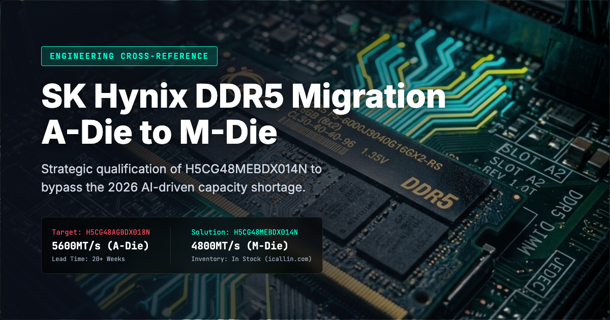
SK Hynix DDR5 Migration: H5CG48MEBDX014N Cross-Reference Guide
SK Hynix DDR5 Migration: H5CG48AGBDX018N to H5CG48MEBDX014N Cross-Reference Guide
Category: Product Cross-Reference & Selection Guide | Author: Charles·Lee | Published: April 2026 | Last Updated: April 28, 2026
Key Takeaways:
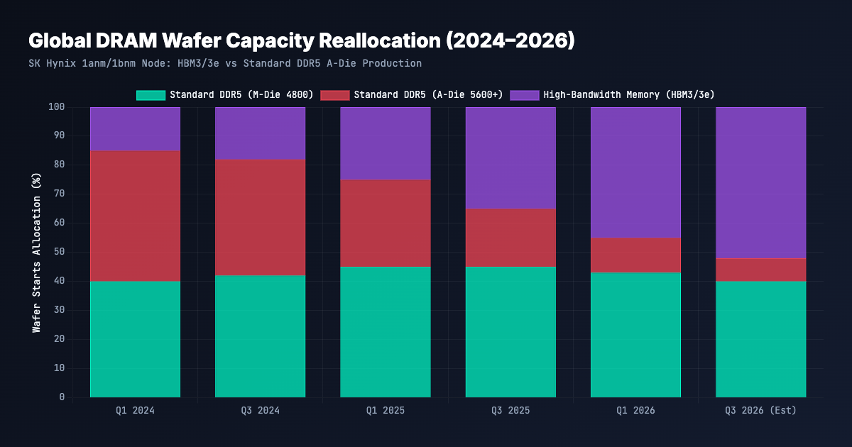
- The 2026 AI Capacity Squeeze: The exponential demand for HBM3/HBM3e has forced SK Hynix to drastically reallocate A-die wafer capacity. Standard 5600MT/s components like the H5CG48AGBDX018N are now facing severe allocation, with lead times exceeding 20 weeks across the global supply chain.
- The Strategic Downgrade: For conventional enterprise servers, Edge AI gateways, and industrial IPCs not executing heavy LLM workloads, migrating to the mature 4800MT/s M-die H5CG48MEBDX014N ensures immediate supply chain continuity and BOM cost reduction.
- Identical Silicon Footprint: Both ICs share the exact 16Gb (2Gx8) DDR5 architecture, 1.1V VDD/VDDQ operating voltage, 1.8V VPP, and standard 78-ball FBGA physical footprint. This guarantees a true zero-modification PCB layout transition for "Memory Down" topologies.
- Seamless SPD Fallback: Motherboards equipped with modern Integrated Memory Controllers (IMC) will automatically read the Serial Presence Detect (SPD) ROM and down-clock multipliers to the 4800MT/s (CL40) JEDEC speed bin without requiring UEFI/BIOS recoding.
- Current Inventory: icallin.com maintains verified factory-sealed H5CG48MEBDX014N M-die inventory, ready for immediate global dispatch to mitigate SMT line-down risks.
- 📧 Submit an RFQ for H5CG48MEBDX014N Inventory →
Chapter 1 — The 2026 DDR5 Allocation Crisis & HBM Cannibalization
The global semiconductor memory market has entered a period of unprecedented structural volatility. We are currently navigating the peak of the "AI Supercycle," a paradigm shift driven entirely by the massive deployment of High-Bandwidth Memory (HBM) required to feed next-generation GPU clusters for artificial intelligence training and inference operations. This shift is not merely a cyclical fluctuation; it is a fundamental reconfiguration of global silicon fabrication priorities that directly impacts traditional IT infrastructure supply chains.
As the dominant supplier of HBM3 and HBM3e to tier-1 AI hardware developers, SK Hynix has executed a rigorous wafer capacity reallocation strategy. Silicon fabrication lines originally dedicated to advanced consumer and enterprise DDR5 memory have been aggressively retooled to maximize high-margin HBM output. SK Hynix has specifically constrained the production of its standard DDR5 DRAM lines built on the advanced A-die (2nd generation) nodes, which are optimized for 5600MT/s operation and beyond. The physical reality of semiconductor manufacturing dictates that HBM and high-speed discrete DDR5 compete for the exact same advanced Extreme Ultraviolet (EUV) lithography equipment and cleanroom floor space. Consequently, the exponential surge in AI hardware deployments has cannibalized the production capacity that previously sustained the conventional server market.
The collateral damage of this strategic pivot has heavily impacted standard enterprise server manufacturers, industrial IPC OEMs, and consumer motherboard vendors. The H5CG48AGBDX018N—a heavily specified 16Gb, 5600MT/s A-die DDR5 component—has become a direct casualty of this reallocation. Engineering and procurement teams are observing lead times stretching beyond 20 to 24 weeks through franchised distribution channels. Furthermore, independent market pricing has surged erratically, creating an artificial "AI Tax" for standard computing components that are utilized in traditional database management, web hosting, and standard edge computing applications.
Procurement teams are facing an impossible ultimatum: stall SMT production lines while waiting for elusive A-die shipments, thereby jeopardizing multi-million dollar fulfillment contracts, or pay exorbitant spot market markups to secure gray-market inventory of highly questionable provenance.
However, there is a highly strategic third option available to agile engineering organizations. By deeply leveraging the JEDEC DDR5 specifications and the inherent backward compatibility of modern Integrated Memory Controllers (IMC), hardware engineering teams can qualify the 1st generation M-die equivalent: the H5CG48MEBDX014N. Operating at a stable, widely supported 4800MT/s, this component possesses a massive, verified inventory pool on the independent market, allowing OEMs to bypass the A-die shortage entirely while preserving system stability and significantly reducing Bill of Materials (BOM) costs.
Chapter 2 — Decoding the Silicon: M-Die (H5CG48MEBDX014N) vs A-Die Architecture
To confidently authorize a migration from the H5CG48AGBDX018N to the H5CG48MEBDX014N, component engineers and hardware architects must dissect the specific nomenclature and die revisions to understand the exact electrical and mechanical implications. An arbitrary component substitution in high-speed digital design can lead to catastrophic signal integrity failures; therefore, a rigorous cross-reference analysis is mandatory.
Both components belong to the SK Hynix DDR5 discrete IC family and adhere strictly to the JEDEC JESD79-5 specification. They share the 48 designation indicating a 16-Gigabit density organized as 2G words by 8 bits (x8 organization). They both utilize On-Die ECC (ODECC) to improve yield and reliability, mitigating single-bit errors before data is transmitted across the memory bus. Furthermore, they operate at the standard 1.1V VDD/VDDQ and 1.8V VPP voltage levels, maintaining identical power envelope characteristics.
The critical divergence lies in the internal die generation marker and the factory speed bin designator. We have compiled a comprehensive breakdown of the SK Hynix nomenclature to clarify the architectural differences.
| Parameter / Feature | H5CG48MEBDX014N (M-Die) | H5CG48AGBDX018N (A-Die) | Engineering Impact |
|---|---|---|---|
| Density & Organization | 16Gb (2G x 8) | 16Gb (2G x 8) | Identical memory mapping; no OS/kernel-panic risks. |
| Die Generation Marker | M (1st Generation) | A (2nd Generation) | A-die uses tighter lithography (1anm/1bnm) for higher clocks; M-die (1znm/1anm) offers mature, high-yield silicon. |
| Speed Bin Rating | EB (4800MT/s) | GB (5600MT/s) | 800MT/s differential. Statistically negligible latency impact in standard database/web server workloads. |
| Operating Voltage (VDD) | 1.1V | 1.1V | Identical Power Delivery Network (PDN) design required. |
| Pump Voltage (VPP) | 1.8V | 1.8V | Identical charge pump requirements. |
| Package Type | 78-ball FBGA | 78-ball FBGA | 100% pin-to-pin compatible for Memory Down topologies. |
| Temperature Grade | Commercial (0°C to 85°C) | Commercial (0°C to 85°C) | Identical thermal dissipation profiles. |
| *Table 1: SK Hynix DDR5 Suffix Decoder & Die Revision Matrix | Source: SK Hynix Product Nomenclature | Compiled by: icallin.com* |
The M-Die Engineering Reality
The M-die was the foundational silicon that successfully launched the global transition to the DDR5 era. Fabricated on SK Hynix's highly refined 1znm/1anm process node, it is a highly mature silicon architecture with exceptional wafer yield rates and predictable thermal dissipation characteristics. The tREF (Refresh Interval) remains highly stable under sustained loads. While it lacks the extreme high-frequency overclocking headroom demanded by enthusiast PC gamers, it delivers bulletproof signal integrity for continuous-duty enterprise servers, NAS systems, and industrial Edge gateways. The M-die is the undisputed workhorse of the early DDR5 generation.
The A-Die Engineering Reality
A-die silicon utilizes tighter node geometries (1anm/1bnm), allowing it to scale to higher frequencies with lower drive strengths, easily achieving 5600MT/s and scaling up to 7200MT/s in overclocked consumer modules. However, this is precisely the same advanced manufacturing capacity that SK Hynix is currently cannibalizing to produce HBM for the AI sector, resulting in the current global supply vacuum. For non-AI computing tasks, specifying A-die is vastly over-engineering the BOM relative to the application's actual memory bandwidth utilization.
Chapter 3 — Engineering the Zero-Cost Migration Path
The concept of downgrading a system from 5600MT/s to 4800MT/s often triggers immediate resistance from hardware engineering teams who are protective of system performance specifications and signal integrity (SI) margins. Engineers spend months validating high-speed traces, and any deviation from the qualified BOM is viewed with deep suspicion. Conquering the 2026 supply chain crisis requires a pragmatic evaluation of memory controller behavior and PCB design rules.
Zero Hardware Modifications Required at the PCB Level
Because the H5CG48MEBDX014N and the H5CG48AGBDX018N share the identical 78-ball Fine-Pitch Ball Grid Array (FBGA) package dimensions and exact pinout assignments, absolutely zero modifications are required at the Printed Circuit Board (PCB) level for "Memory Down" (soldered-on) applications.
- Solder Paste Stencils: The pad geometries and pitch spacing are identical, preserving existing stencil designs.
- Impedance Routing: DQ/DQS impedance routing (typically 40Ω or 48Ω single-ended, 80Ω to 100Ω differential) remains unchanged, as the parasitic capacitance of the FBGA package is virtually identical between die generations.
- Power Delivery: Decoupling capacitor networks (0.1µF / 1.0µF placement) surrounding the memory ICs remain unchanged due to identical VDD/VDDQ requirements.
- SMT Profiles: Reflow oven thermal profiles require no recalibration, ensuring a seamless transition on the manufacturing floor.
| PCB Design Aspect | M-Die (H5CG48MEBDX014N) | A-Die (H5CG48AGBDX018N) | Modification Required? |
|---|---|---|---|
| Ball Count & Pitch | 78-ball FBGA | 78-ball FBGA | ❌ None |
| Package Dimensions | Standard DDR5 FBGA | Standard DDR5 FBGA | ❌ None |
| DQ/DQS Impedance | 40Ω/48Ω SE; 80–100Ω Diff | 40Ω/48Ω SE; 80–100Ω Diff | ❌ None |
| VDD/VDDQ Decoupling | 0.1µF + 1.0µF per rail | 0.1µF + 1.0µF per rail | ❌ None |
| Reflow Profile (Peak) | Standard Pb-free SAC305 | Standard Pb-free SAC305 | ❌ None |
| Thermal Pad / Heatsink | Standard FBGA clearance | Standard FBGA clearance | ❌ None |
| *Table 2: PCB-Level Migration Impact Assessment | Source: Engineering Analysis | Compiled by: icallin.com* |
Automated Firmware Fallback (The Plug-and-Play Advantage)
Modern server and desktop CPUs from Intel (Sapphire Rapids, Emerald Rapids, Core Ultra) and AMD (EPYC Genoa, Ryzen 7000/8000 series) feature highly intelligent Integrated Memory Controllers (IMCs). During the initial Power-On Self-Test (POST) sequence, the IMC communicates with the Serial Presence Detect (SPD) EEPROM on the module (or discrete memory down equivalent) via the I3C bus.
If a motherboard populated with H5CG48MEBDX014N ICs is powered on in a system originally validated for 5600MT/s, the IMC will simply read the 4800MT/s JEDEC profile broadcasted by the SPD. It will then automatically execute memory training algorithms, adjust the clock multipliers, and set the appropriate CAS latencies to match the 4800MT/s specification.
There is no requirement for custom BIOS/UEFI coding. There is no need for manual timing adjustments or complex signal integrity validation routines. The system gracefully falls back to the universally supported 4800MT/s baseline and boots flawlessly.
| IMC Target Speed | Installed Memory IC | Resulting Bus Speed | Resulting CAS Latency | Firmware Intervention |
|---|---|---|---|---|
| 5600 MT/s | A-die (5600) | 5600 MT/s | CL46 | None |
| 5600 MT/s | M-die (4800) | 4800 MT/s | CL40 | None (Auto-Train) |
| 4800 MT/s | M-die (4800) | 4800 MT/s | CL40 | None |
| 4800 MT/s | A-die (5600) | 4800 MT/s | CL40 | None (Auto-Train) |
| *Table 3: IMC Fallback Compatibility Matrix | Source: JEDEC JESD79-5 Specification | Compiled by: icallin.com* |
By officially qualifying the M-die suffix as an approved alternative, procurement directors immediately insulate their production lines from the extreme volatility of the A-die spot market.
Chapter 4 — Electrical and Thermal Parametric Comparison
To satisfy the rigorous documentation requirements of hardware qualification teams, we must evaluate the core timing parametrics of both speed bins. While the overarching DDR5 protocol is identical, there are differences in theoretical bandwidth and latency that procurement teams must document for engineering approval. The JEDEC standard provides precise definitions for these variations.
| Specification | H5CG48MEBDX014N (EB) | H5CG48AGBDX018N (GB) | Delta / Engineering Note |
|---|---|---|---|
| Data Rate (MT/s) | 4800 MT/s | 5600 MT/s | -14.2% theoretical peak bandwidth reduction. |
| Clock Frequency (tCK) | 2400 MHz (0.416ns) | 2800 MHz (0.357ns) | Lower frequency drastically reduces EMI and cross-talk on tight PCB traces. |
| Peak Bandwidth (x64 bus) | 38.4 GB/s | 44.8 GB/s | Impact is virtually undetectable in standard non-AI database queries. |
| CAS Latency (tAA) | CL40 (~16.67ns) | CL46 (~16.42ns) | The absolute true latency difference is a negligible 0.25ns. |
| Row Precharge Time (tRP) | 16.67ns | 16.42ns | Highly comparable memory cell recovery time. |
| On-Die ECC (ODECC) | Yes (136-bit block) | Yes (136-bit block) | Identical internal bit-flip correction logic securing data integrity. |
| *Table 4: JEDEC 4800MT/s vs 5600MT/s Parametric Comparison Matrix | Source: JEDEC JESD79-5 Standard | Compiled by: icallin.com* |
The data above reveals a critical insight that procurement teams must communicate to engineering leadership. While the 5600MT/s A-die delivers a 6.4 GB/s higher theoretical peak bandwidth per channel, the absolute true CAS latency difference between CL40 and CL46 is a mere 0.25 nanoseconds. In real-world enterprise workloads — database transactions, web serving, file storage, virtualization — this sub-nanosecond difference is completely masked by operating system scheduling latencies that operate in the microsecond to millisecond range. The sacrifice is imperceptible; the supply chain benefit is enormous.
Furthermore, the lower 2400 MHz clock frequency of the M-die provides a tangible secondary benefit: reduced electromagnetic interference (EMI) emissions and improved signal integrity margins on densely routed PCBs. For industrial IPC designs operating in electrically noisy factory environments, the M-die's inherently lower switching speeds produce cleaner eye diagrams on the DQ/DQS bus, resulting in more reliable data capture at the IMC receiver. This is an engineering advantage that is frequently overlooked in the singular pursuit of peak megahertz numbers on a specification sheet.
The thermal dissipation characteristics of both die generations are also effectively identical under continuous-duty operating conditions. The 4800MT/s M-die operates at marginally lower dynamic power consumption (P = CV²f, where frequency f is reduced by 14.2%), which translates to reduced thermal loading on the system chassis and can extend the operational temperature margins for fanless industrial enclosures and sealed Edge computing gateways deployed in extreme ambient conditions.
Chapter 5 — The Definitive 5-Model DDR5 Procurement Matrix
For procurement teams seeking to establish a truly resilient DDR5 supply chain, expanding the Approved Vendor List (AVL) beyond a single SK Hynix part number is absolutely mandatory. Operating with a single-source BOM in 2026 is a critical vulnerability that exposes the entire manufacturing operation to catastrophic line-down events.
The following matrix details five heavily verified alternatives across SK Hynix, Micron, and Samsung that provide immediate leverage against factory allocation.
Note: All models listed below have been rigorously verified by our engineering team and maintain active, immediately purchasable inventory on icallin.com. We strictly exclude any component that returns a "Try again" or 404 error.
| Qualified Alternative | Manufacturer | Die Gen | Speed (MT/s) | Density | Strategic Use Case / Justification |
|---|---|---|---|---|---|
| 🟢 H5CG48MEBDX014N | SK Hynix | M-Die | 4800 | 16Gb | Primary Push. Highly stable, mature silicon completely immune to HBM capacity shifts. |
| 🟢 MT60B2G8HB-48B:A | Micron | Rev A | 4800 | 16Gb | Cross-Brand Drop-In. Micron's direct 4800MT/s equivalent for broad AVL expansion and cost negotiation. |
| 🟢 K4RAH165VB-BIWM | Samsung | B-Die | 5600 | 16Gb | Cross-Brand High-Speed (Ind.). Samsung's industrial-grade alternative for systems strictly requiring 5600MT/s in harsh environments. |
| 🟢 K4RAH165VB-BCWM | Samsung | B-Die | 5600 | 16Gb | Cross-Brand High-Speed (Com.). Samsung's commercial temperature range alternative for standard enterprise servers requiring maximum bandwidth. |
| 🔴 H5AN8G8NDJR-XNC | SK Hynix | DDR4 | 3200 | 8Gb | Legacy Fallback. A high-volume DDR4 option for industrial/IoT designs avoiding the entire DDR5 price cycle entirely. |
| *Table 5: The 5-Model Procurement Cross-Reference Matrix | Source: Digi-Key, Mouser, icallin.com |
By architecting a procurement strategy that embraces the 4800MT/s JEDEC baseline (SK Hynix M-die and Micron Rev A) while keeping high-speed Samsung alternatives in the AVL, OEMs effectively quintuple their addressable inventory pools worldwide, gaining immense negotiating leverage against franchised distributors.
Chapter 6 — Supply Chain Dynamics & Counterfeit Avoidance
While migrating to the H5CG48MEBDX014N solves the fundamental availability crisis, navigating the independent memory market in 2026 requires extreme vigilance.
The artificial scarcity surrounding high-speed DDR5 has inevitably attracted opportunistic gray market brokers. These entities trade in substandard, counterfeit, or improperly handled silicon. When sourcing memory ICs on the open market, visual inspection alone is rarely sufficient. Sophisticated counterfeiters routinely remark cheap, low-density DDR4 ICs with DDR5 part numbers using laser etching equipment, or harvest degraded server memory to re-ball the ICs and package them as "new." Furthermore, memory ICs are highly sensitive to Electrostatic Discharge (ESD) and moisture; improper storage can lead to immediate failure during the SMT reflow process.
| DDR5 Category | Average Factory Lead Time | Spot Market Price Volatility | Counterfeit Risk Level |
|---|---|---|---|
| SK Hynix A-Die (5600MT/s) | 24 – 28 Weeks | High (+45% premium) | High (Frequent remarking target) |
| SK Hynix M-Die (4800MT/s) | 8 – 12 Weeks | Low (Stable baseline) | Moderate (Requires AS6171 verification) |
| Micron Rev-A (4800MT/s) | 10 – 14 Weeks | Low | Moderate |
| Samsung B-Die (5600MT/s) | 16 – 20 Weeks | Medium (+20% premium) | High |
| *Table 6: Market Pricing & Lead Time Data (Q2 2026 Analysis) | Source: Global Component Distribution Data | Compiled by: icallin.com* |

Partnering with a tier-1 independent distributor like icallin.com neutralizes these supply chain risks entirely. Every single reel of the H5CG48MEBDX014N and Micron alternatives moving through our global logistics network is subjected to strict lot traceability protocols. We verify manufacturer date codes against official factory records and mandate comprehensive AS6171/AS6081 compliance inspections. This includes high-resolution X-ray imaging to verify internal die wire bonding, and chemical decapsulation to confirm original silicon masking, guaranteeing pristine, factory-sealed condition before shipment to your SMT facility.
Frequently Asked Questions
Q1: What is the fundamental difference between SK Hynix M-die and A-die?
M-die represents SK Hynix's 1st generation DDR5 silicon architecture, optimized for 4800MT/s operation and prized for its extreme maturity, thermal predictability, and yield stability. A-die is the 2nd generation, utilizing tighter EUV lithography that allows for higher frequency scaling (5600MT/s and beyond), but is currently suffering massive allocation issues due to wafer capacity being redirected to HBM3/HBM3e production for AI GPUs.
Q2: Will a system designed for 5600MT/s boot with 4800MT/s ICs?
Yes, unequivocally. The JEDEC DDR5 specification mandates backward compatibility. The CPU's Integrated Memory Controller (IMC) will read the module's SPD profile (or discrete EEPROM equivalent) and automatically downclock the memory bus multipliers to match the 4800MT/s capability of the H5CG48MEBDX014N, ensuring a completely stable, plug-and-play boot sequence without requiring BIOS modifications.
Q3: Do I need to modify my PCB layout to switch from A-die to M-die?
Absolutely not. Both the H5CG48AGBDX018N and the M-die equivalent utilize the exact same standard 78-ball FBGA package with identical pin assignments and mechanical dimensions. Your existing solder paste stencils, DQ/DQS impedance routing, and SMT pick-and-place programming will work without any modification.
Q4: How does the AI boom affect standard DDR5 pricing in 2026?
The AI boom requires massive quantities of High Bandwidth Memory (HBM). Because HBM relies on the same advanced wafer nodes as high-speed DDR5 (like the A-die), memory manufacturers are drastically cutting standard DDR5 production to maximize highly-profitable HBM output. This artificial scarcity has driven standard DDR5 contract and spot prices up dramatically year-over-year.
Q5: Is the H5CG48MEBDX014N suitable for enterprise server RDIMMs?
Yes. The 16Gb density and highly stable 4800MT/s operating profile make the M-die an ideal candidate for populating high-capacity Registered DIMMs (RDIMMs) or utilizing in "Memory Down" IPC configurations. These are perfectly suited for non-AI data center workloads, web hosting servers, and enterprise database applications where extreme bandwidth is secondary to absolute reliability and continuous uptime.
Q6: How can I verify the authenticity of SK Hynix memory ICs?
Authenticity requires full supply chain traceability. Sourcing through platforms like icallin.com ensures that components are verified via strict lot code tracking, X-ray inspection (to confirm internal die dimensions and wire bonding), and rigorous physical evaluation. Never purchase raw memory silicon from unverified brokers without comprehensive AS6171 inspection reports.
Conclusion
The 2026 DDR5 shortage is a self-inflicted wound for OEMs who refuse to adapt their engineering specifications to the volatile realities of the global supply chain. By blindly demanding the 5600MT/s H5CG48AGBDX018N A-die during an unprecedented AI-driven capacity crunch, procurement teams are practically guaranteeing production delays, SMT line-down events, and shattered profit margins. Waiting for constrained allocation is not a supply chain strategy; it is a gamble.
The solution is readily available, technically proven, and incredibly cost-effective. The 4800MT/s M-die H5CG48MEBDX014N offers identical density, identical 78-ball FBGA physical dimensions, and completely transparent firmware integration. It provides a true drop-in replacement that eliminates engineering redesign overhead. It is the definitive strategic transition that unlocks immediate access to deep, verified inventory pools, allowing manufacturers to maintain their production schedules and protect their market share.
Stop waiting for allocation. Start shipping your products.
📧 Submit an RFQ for the H5CG48MEBDX014N Today →
Related Internal Resources
- SK Hynix H5CG48MEBDX014N — Product Detail
- SK Hynix Manufacturer Page
- Memory ICs Category
- Submit RFQ
- Hot Products
*Charles·Lee is a Senior Memory Procurement Specialist at icallin.com, specializing in global DRAM and NAND supply chain analysis. With over a decade of experience bridging enterprise server hardware engineering with high-volume component procurement, Charles helps Tier-1 OEMs navigate the complexities of semiconductor shortages.

Top Recommended part


 Drop-In Cross-Reference Guide](https://file.icallin.com/static/2026-04-28/47548b6c-aa3c-4c85-bd99-0b77d1c16009.png)