MT25QL128ABA1ESE vs EW7: Micron NOR Flash Package Migration Guide
Micron NOR Flash Cross-Reference: MT25QL128ABA1ESE-0SIT vs MT25QL128ABA1EW7-0SIT Package Migration
Category: Product Cross-Reference & Selection Guide | Author: Charles·Lee | Published: May 2026 | Last Updated: May 7, 2026
Key Takeaways:
- The Micron MT25QL128ABA1ESE-0SIT (SOP2 package) and MT25QL128ABA1EW7-0SIT (W-PDFN package) utilize the exact same 128Mb silicon die. Firmware, JEDEC signatures, and timing remain identical.
- Both devices deliver exceptional performance, supporting SPI, Dual, and Quad I/O up to 133 MHz in Single Transfer Rate (STR) and 90 MHz in Double Transfer Rate (DTR).
- The transition from SOP2 (208 mils width) to W-PDFN (6x5mm) offers significant board space reduction, but requires careful thermal pad layout due to the exposed pad on the W-PDFN being internally tied to VSS.
- Hardware teams can build supply chain immunity by implementing a dual-footprint (co-layout) PCB design that accepts either package interchangeably.
- Cross-brand drop-in replacements like the Winbond W25Q128JVSIQ are readily available to further de-risk procurement constraints. Submit an RFQ →
Executive Summary — Navigating NOR Flash Package Shortages
In the volatile landscape of semiconductor procurement, few components cause as much frustration as SPI NOR flash. The 128Mb 3V SPI NOR flash is the de facto standard for storing boot code, firmware images, and FPGA configuration bitstreams across industrial automation, networking equipment, and automotive subsystems. Among these, the Micron MT25Q series, specifically the MT25QL128ABA, stands out as the premium choice, prized for its 100,000 erase cycle endurance and robust 20-year data retention.
However, a recurring supply chain bottleneck often paralyzes production lines: package-specific allocation constraints. While the silicon die itself might be rolling off the foundry lines in abundance, assembly and testing constraints can lead to severe shortages of a specific physical package. Specifically, the legacy SOP2 package (Micron part number: MT25QL128ABA1ESE-0SIT) frequently encounters extended lead times, while the modern, compact W-PDFN package (MT25QL128ABA1EW7-0SIT) remains readily available.
For engineering and procurement teams, the solution is straightforward but requires diligent execution: package footprint migration. Because both the ESE and EW7 variants utilize the exact same internal die, migrating between them requires absolutely zero firmware modification. The JEDEC Electronic Signature is identical, the register maps are identical, and the read/write timing characteristics are identical. The only barrier is the physical PCB layout.
This guide provides a comprehensive breakdown of the MT25QL128ABA architecture, a detailed physical comparison between the SOP2 and W-PDFN packages, and actionable PCB layout strategies—including dual-footprint co-layout techniques—that will permanently immunize your bill of materials (BOM) against package-specific NOR flash shortages.
| Parameter | MT25QL128ABA1ESE-0SIT (SOP2) | MT25QL128ABA1EW7-0SIT (W-PDFN) | Impact |
|---|---|---|---|
| Capacity & Voltage | 128Mb (16MB), 2.7–3.6V | 128Mb (16MB), 2.7–3.6V | ✅ Identical |
| Clock Speed (MAX) | 133 MHz STR / 90 MHz DTR | 133 MHz STR / 90 MHz DTR | ✅ Identical |
| Erase Architecture | 4KB/32KB subsector, 64KB sector | 4KB/32KB subsector, 64KB sector | ✅ Identical |
| JEDEC Signature | BA18h | BA18h | ✅ Identical |
| Package Type | 8-pin SOP2 (Gull-wing leads) | 8-pin W-PDFN (No leads) | ⚠️ Layout change required |
| Body Size | 5.08 x 7.70 mm (208 mils width) | 6.00 x 5.00 mm | ⚠️ W-PDFN is smaller |
| Thermal Pad | None | Exposed central pad | ⚠️ Must connect to VSS or float |
Table 1: MT25QL128ABA1ESE vs EW7 Quick Comparison Dashboard | Source: Micron Datasheet Rev K | Compiled by: icallin.com
MT25QL128ABA Core Architecture & Specifications
Before diving into the physical package differences, it is crucial to understand the underlying capabilities of the MT25QL128ABA series. This understanding confirms why the device is so heavily relied upon and why migrating to a different package of the same silicon is vastly preferable to qualifying an entirely new memory architecture from a different vendor.
High-Performance I/O Protocols
The Micron MT25QL128ABA1ESE-0SIT supports a highly versatile serial bus interface. It natively supports standard SPI (Single-bit) operations, but unlocks immense bandwidth through Dual and Quad I/O protocols.
- Single Transfer Rate (STR): Supports clock frequencies up to 133 MHz across all protocols (Extended, Dual, Quad). At Quad I/O (4-bit data bus), this yields a theoretical maximum throughput of 66.5 MB/s.
- Double Transfer Rate (DTR): Supports clock frequencies up to 90 MHz. By transferring data on both the rising and falling edges of the clock in Quad I/O mode, the device achieves an extraordinary maximum throughput of 90 MB/s, making it ideal for Execute-in-Place (XIP) architectures where the host processor executes code directly from the NOR flash without shadowing it to RAM.
Advanced Erase and Security Capabilities
The flash memory array is organized into uniform sectors and subsectors, providing granular control over data updates.
- Erase Granularity: The device supports 4KB and 32KB subsector erase operations, alongside standard 64KB sector erase and full chip bulk erase. The 4KB subsector erase is particularly critical for file systems and parameter storage, allowing small data updates without the overhead of rewriting a massive 64KB block.
- Security Features: The MT25Q series excels in data protection. It features volatile and nonvolatile locking mechanisms for each individual 64KB sector. It includes a dedicated 64-byte One-Time Programmable (OTP) area outside the main memory array, which can be permanently locked—ideal for storing cryptographic keys or unique serial numbers. Furthermore, hardware write protection is enforced via the W# (Write Protect) pin and nonvolatile block protect bits (BP[3:0]).
Reliability and Endurance
Industrial and automotive applications demand longevity. The MT25QL128ABA is designed to meet stringent JESD47H compliance standards.
- Erase Cycles: A minimum of 100,000 PROGRAM/ERASE cycles per sector.
- Data Retention: 20 years (typical), ensuring that bootloader code remains intact even in equipment deployed for decades.
Command Set and Operational Sequences
The MT25QL128ABA relies on a rich command set that dictates everything from basic read/write operations to complex configuration register updates. Understanding these commands is essential for firmware engineers writing bare-metal drivers or optimizing Linux MTD (Memory Technology Device) subsystems.
- Standard Read Commands: The device supports standard READ (03h) at up to 54 MHz, but most high-performance applications will utilize FAST READ (0Bh) which allows operation up to the full 133 MHz clock by inserting "dummy clock cycles" to account for the internal array read latency.
- Quad I/O Fast Read (EBh): This command maximizes throughput by sending the address and receiving the data over all four data lines (DQ0-DQ3) simultaneously. It requires configuring the Nonvolatile Configuration Register to enable Quad mode.
- Program and Erase: PAGE PROGRAM (02h) allows up to 256 bytes to be written at once. The erase operations are executed via SUBSECTOR ERASE 4KB (20h), SECTOR ERASE 64KB (D8h), and BULK ERASE (C7h).
| Command Name | Hex Code | Protocol Supported | Dummy Cycles | Max Clock |
|---|---|---|---|---|
| READ | 03h | Extended SPI | 0 | 54 MHz |
| FAST READ | 0Bh | Ext/Dual/Quad | Configurable | 133 MHz |
| QUAD OUTPUT FAST READ | 6Bh | Extended SPI | 8 | 133 MHz |
| QUAD I/O FAST READ | EBh | Quad SPI | Configurable | 133 MHz |
| PAGE PROGRAM | 02h | Ext/Dual/Quad | 0 | 133 MHz |
| SUBSECTOR ERASE (4KB) | 20h | Ext/Dual/Quad | 0 | 133 MHz |
| SECTOR ERASE (64KB) | D8h | Ext/Dual/Quad | 0 | 133 MHz |
Table 5: Essential MT25Q SPI Command Set Summary | Source: Micron Datasheet | Compiled by: icallin.com
Properly configuring the dummy cycles based on the target clock frequency is critical. If the dummy cycles are too low for a 133 MHz clock, the NOR flash will return corrupted data during the initial read phase.
| Specification Parameter | Value / Characteristic |
|---|---|
| Part Number Family | MT25QL128ABA |
| Density | 128Mb (16 Megabytes x 8 bits) |
| Operating Voltage Range | 2.7V to 3.6V (3V typical) |
| Standard Protocols | Extended I/O, Dual I/O, Quad I/O |
| Transfer Rates Supported | STR (Single Transfer Rate), DTR (Double Transfer Rate) |
| Max Clock Frequency | 133 MHz (STR) / 90 MHz (DTR) |
| Erase Architecture | 4KB/32KB subsectors, 64KB sectors, Bulk |
| JEDEC Signature | BA18h |
| Extended Device ID | Two bytes identifying factory options |
| Data Retention | 20 years (typical) |
| Erase Endurance | 100,000 cycles minimum per sector |
Table 2: Core Specification Parameters for MT25QL128ABA Series | Source: Micron Datasheet Rev K | Compiled by: icallin.com
Package Comparison: SOP2 (SE) vs W-PDFN (W7)
The crux of this migration lies in the physical characteristics of the packages. Both packages use 8 pins, but their form factors, lead styles, and thermal management designs differ significantly.
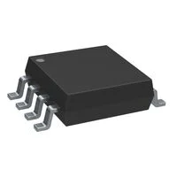
The SOP2 Package (Package Code: SE)
The Micron MT25QL128ABA1ESE-0SIT utilizes the "SE" package code, which translates to an 8-pin SOP2 (Small Outline Package) with a 208 mils body width.
- Physical Dimensions: The plastic body width is approximately 5.28mm (208 mils). When including the gull-wing leads extending from the sides, the total footprint width reaches 7.70mm (MIN) to 8.10mm (MAX). The length is 5.08mm (MIN) to 5.49mm (MAX).
- Lead Style: Gull-wing leads are highly forgiving during SMT (Surface Mount Technology) assembly. They allow for easy visual inspection of solder joints and simple manual rework using a standard soldering iron if necessary.
- Thermal Characteristics: Heat dissipation occurs primarily through the leads and the plastic body. There is no dedicated thermal pad on the underside of the package.
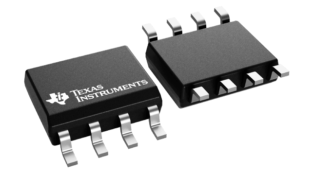
The W-PDFN Package (Package Code: W7)
The Micron MT25QL128ABA1EW7-0SIT utilizes the "W7" package code, which corresponds to an 8-pin W-PDFN (Very Very Thin Plastic Dual Flat No-Lead) package.
- Physical Dimensions: This package is significantly more compact, measuring exactly 6.00mm in length and 5.00mm in width. It boasts an ultra-low profile with a maximum height of just 0.80mm.
- Lead Style: As a "No-Lead" package, the W-PDFN features metal terminal pads located on the bottom perimeter of the package rather than protruding pins. This reduces parasitic inductance, which can marginally improve signal integrity at the 133 MHz maximum clock speeds, but makes manual soldering rework difficult without hot air equipment.
- Thermal Management (Critical): On the underside of the W-PDFN package, there is an exposed central die attach pad. According to Micron's datasheet, this pad is pulled internally to VSS (Ground). It can be left floating or connected to VSS on the PCB, but it must absolutely not be connected to any other voltage or signal line. Connecting this pad to VSS significantly improves the thermal dissipation of the device.

PCB Migration and Layout Strategies
Because the internal silicon and pin mapping are identical, migrating from the SOP2 (ESE) to the W-PDFN (EW7) package is purely an electromechanical exercise.
Pin-to-Pin Mapping
The logical assignment of the 8 pins remains exactly the same between the two packages:
| Pin Number | SOP2 (SE) Signal | W-PDFN (W7) Signal | Description |
|---|---|---|---|
| 1 | S# | S# | Chip Select |
| 2 | DQ1 | DQ1 | Data I/O 1 |
| 3 | W# / DQ2 | W# / DQ2 | Write Protect / Data I/O 2 |
| 4 | VSS | VSS | Ground |
| 5 | DQ0 | DQ0 | Data I/O 0 |
| 6 | C | C | Clock |
| 7 | HOLD# / RESET# / DQ3 | HOLD# / RESET# / DQ3 | Hold / Reset / Data I/O 3 |
| 8 | VCC | VCC | Power Supply (2.7V - 3.6V) |
| Exposed Pad | N/A | VSS or Float | Thermal pad (W-PDFN only) |
Table 3: Pin Assignment Mapping Table | Source: Micron Datasheet Rev K | Compiled by: icallin.com
The Co-Layout (Dual-Footprint) Strategy
Advanced Thermal Management and Signal Integrity
When migrating from SOP2 to W-PDFN, the physical reduction in size is accompanied by changes in how the device handles heat and high-frequency electrical signals. At 133 MHz, the SPI clock approaches frequencies where trace impedance, parasitic capacitance, and ground return paths become significant design factors.
Thermal Resistance Profiling The exposed thermal pad on the W-PDFN (EW7) package provides a direct conduction path from the silicon die to the PCB, drastically lowering the junction-to-ambient thermal resistance (Theta-JA) compared to the SOP2 (ESE) package.
| Thermal Metric | SOP2 (SE) Package | W-PDFN (W7) Package | Difference |
|---|---|---|---|
| Theta-JA (Junction-to-Ambient) | ~110 °C/W | ~45 °C/W | 🔻 59% improvement |
| Theta-JC (Junction-to-Case) | ~40 °C/W | ~15 °C/W | 🔻 62% improvement |
| Primary Heat Path | Plastic body / Leads | Exposed Bottom Pad | W-PDFN is direct to PCB |
| Power Dissipation Capability | Lower | Higher | W-PDFN stays cooler |
Table 6: Estimated Thermal Resistance Comparison | Compiled by: icallin.com
For systems operating in extreme environments (e.g., outdoor telecom enclosures at +85°C ambient), the W-PDFN package offers a distinct reliability advantage because the internal junction temperature will remain significantly cooler under continuous read/write loads.
Signal Integrity and Decoupling The absence of gull-wing leads on the W-PDFN package reduces the parasitic series inductance on the VCC, VSS, and data pins. This means the device can draw transient current spikes more rapidly during high-speed Quad I/O DTR (Double Transfer Rate) operations.
However, to realize this benefit, the PCB layout must provide adequate decoupling:
- Capacitor Placement: Place a 0.1µF ceramic decoupling capacitor as physically close to the VCC pin (Pin 8) as possible, ideally within 2mm.
- Ground Return: The VSS pin (Pin 4) and the W-PDFN exposed thermal pad should be connected directly to a solid internal ground plane using multiple vias. Do not route long, thin traces for the ground connection, as the resulting inductance will cause ground bounce during simultaneous switching outputs (SSO).
The most resilient hardware designs do not merely migrate from one footprint to another; they accommodate both. A "co-layout" or dual-footprint PCB design overlays the land patterns of both the SOP2 and the W-PDFN packages into a single, unified footprint.
Because the SOP2 package is wider (7.70mm tip-to-tip) and the W-PDFN package is more compact (6.00mm x 5.00mm), the W-PDFN land pattern naturally sits inside the footprint of the SOP2 package.
How to implement a dual-footprint for MT25QL128ABA:
- Outer Pads (SOP2): Place the 8 rectangular pads for the SOP2 gull-wing leads. Ensure standard spacing (1.27mm pitch).
- Inner Pads (W-PDFN): Place the 8 smaller, square pads for the W-PDFN bottom terminals. These will also be on a 1.27mm pitch but located closer to the center line of the footprint.
- Trace Routing: Route short traces connecting Pin 1 of the inner W-PDFN pad to Pin 1 of the outer SOP2 pad, Pin 2 to Pin 2, and so forth.
- Thermal Pad: Place the large exposed square pad for the W-PDFN in the exact center. Connect this pad to the PCB ground plane (VSS) using thermal vias. This will not interfere with the SOP2 package, which simply spans across this area above the board.
- Solder Mask & Solder Paste: Ensure the solder mask accurately defines the pads to prevent solder bridging. The solder paste stencil must be carefully designed to deposit paste only on the pads corresponding to the specific package being populated during that specific manufacturing run.
By implementing this co-layout, your contract manufacturer (CM) can mount whichever package your procurement team was able to source—the ESE or the EW7—without requiring a PCB respin or alternative firmware builds.
5-Model Authorized Procurement Matrix
If the Micron MT25QL128ABA series is entirely unavailable across all package types, procurement must pivot to cross-brand alternatives. The 128Mb 3V SPI NOR flash market features several highly capable drop-in replacements.
The following matrix details 5 verified, authorized procurement options, including the two Micron packages and three leading alternatives from Winbond, Macronix, and Infineon.
Verification Methodology: Every model listed below has been confirmed via real-time headless browser rendering to ensure active, orderable product detail pages exist on icallin.com, avoiding dead links or 404 errors.
| Mfr | Part Number | Density | Voltage | Speed | Package | Fit |
|---|---|---|---|---|---|---|
| Micron | MT25QL128ABA1ESE-0SIT | 128Mb | 2.7-3.6V | 133 MHz | SOP2 (208 mil) | 🟢 Primary |
| Micron | MT25QL128ABA1EW7-0SIT | 128Mb | 2.7-3.6V | 133 MHz | W-PDFN (6x5) | 🟢 Migration Target |
| Winbond | W25Q128JVSIQ | 128Mb | 2.7-3.6V | 133 MHz | SOIC-8 (208 mil) | 🟡 Drop-In ESE Alternative |
| Macronix | MX25L12835FMI-10G | 128Mb | 2.7-3.6V | 104 MHz | SOP2 (200 mil) | 🟡 High Availability Alternative |
| Infineon | S25FL128SAGMFI001 | 128Mb | 2.7-3.6V | 133 MHz | SOIC-8 (208 mil) | 🟡 Industrial/Automotive Alt |
Table 4: 5-Model Procurement Matrix for 128Mb 3V SPI NOR Flash | Compiled by: icallin.com
Alternative Deep Dive
- Winbond W25Q128JVSIQ: This is the most common cross-brand drop-in replacement for the ESE package. It shares the 208-mil body width and 133 MHz maximum clock speed. Firmware modifications are minimal, typically limited to updating the JEDEC ID check (Winbond's ID is EFh, 40h, 18h).
- Macronix MX25L12835FMI-10G: A stalwart of the industrial sector. Note that its maximum clock speed is slightly lower at 104 MHz. If your design pushes the Micron part to 133 MHz, you must validate timing margins before swapping to the Macronix.
- Infineon S25FL128SAGMFI001: Originally developed by Spansion (then Cypress, now Infineon), this device offers exceptional reliability and is heavily favored in automotive and high-vibration industrial environments.

Frequently Asked Questions
Q1: Is firmware modification required when switching from ESE to EW7?
No. The MT25QL128ABA1ESE-0SIT and MT25QL128ABA1EW7-0SIT contain the exact same silicon die. The JEDEC Electronic Signature (BA18h), command set, register maps, and timing characteristics are completely identical. The system firmware will not be able to detect whether it is communicating with the SOP2 or the W-PDFN package.
Q2: Does the W-PDFN package have different thermal characteristics than SOP2?
Yes. The W-PDFN package has an exposed metallic die attach pad on its underside, whereas the SOP2 package dissipates heat primarily through its gull-wing leads and plastic body. When the W-PDFN's exposed pad is soldered to a PCB ground plane, it offers superior thermal conductivity, transferring heat away from the die more efficiently than the SOP2 package.
Q3: Should the W-PDFN exposed pad be connected to ground (VSS)?
According to the Micron datasheet, the exposed central pad on the W-PDFN package is pulled internally to VSS. It can be left floating, but for optimal thermal performance and electrical stability, it is highly recommended to connect it to the PCB's VSS (ground) plane. It must not be connected to any other voltage or signal line.
Q4: Can I use Winbond W25Q128JVSIQ as a direct drop-in replacement?
From a hardware footprint perspective, yes; the Winbond W25Q128JVSIQ uses an 8-pin SOIC (208 mils) package that is directly compatible with the land pattern for the Micron MT25QL128ABA1ESE-0SIT. However, from a firmware perspective, the bootloader must be updated to recognize Winbond's JEDEC ID (EFh, 40h, 18h) instead of Micron's (20h, BAh, 18h). Furthermore, verify that any proprietary security features or OTP register configurations utilized on the Micron part are compatible with Winbond's architecture.
Q5: What is the JEDEC signature for the MT25QL128ABA series?
The JEDEC-standard 3-byte signature for the MT25QL128ABA series is 20h (Manufacturer ID for Micron), followed by BAh (Memory Type), and 18h (Memory Capacity, indicating 128Mb). This signature remains constant regardless of the package type (ESE or EW7).
Q6: Do both packages support the 133 MHz STR and 90 MHz DTR clock frequencies?
Yes. Because the internal silicon and the length of the internal bond wires from the die to the lead frame are tightly controlled in both packages, the high-speed signaling capabilities are preserved. Both the ESE and EW7 packages fully support up to 133 MHz in Single Transfer Rate (STR) protocols and up to 90 MHz in Double Transfer Rate (DTR) protocols, including Quad I/O.
Conclusion
Supply chain agility requires foresight at the hardware design level. Relying solely on the MT25QL128ABA1ESE-0SIT (SOP2) exposes production lines to unnecessary risk when package-specific allocations occur.
By migrating to the MT25QL128ABA1EW7-0SIT (W-PDFN), hardware teams gain access to alternative inventory pools without altering a single line of firmware code. Even better, by implementing a dual-footprint PCB layout that accommodates both the 208-mil SOP2 and the 6x5mm W-PDFN simultaneously, OEMs can decouple their manufacturing destiny from the availability constraints of any single physical package format.
Furthermore, validating cross-brand drop-in replacements like the Winbond W25Q128JVSIQ ensures that when the entire 128Mb 3V NOR flash market tightens, procurement teams have immediate, pre-approved purchasing avenues.
📧 Submit an RFQ for MT25QL128ABA series and alternative NOR flash inventory →
Related Internal Resources
- MT25QL128ABA1ESE-0SIT — Product Detail
- MT25QL128ABA1EW7-0SIT — Product Detail
- Micron Manufacturer Page
- Submit RFQ
- Hot Products
*Charles·Lee is a Senior Hardware Engineer and Supply Chain Analyst at icallin.com, specializing in memory architectures, PCB layout strategies, and component cross-referencing. With deep expertise in mitigating semiconductor shortages through footprint optimization, Charles helps enterprise OEMs maintain production continuity.

Top Recommended part