Samsung LPDDR4 Equivalent: K4FBE3D4HM-GHCL to K4FBE3D4HB-KHCL02V Guide
LPDDR4 Mobile RAM Equivalents: Substituting Samsung K4FBE3D4HM-GHCL with K4FBE3D4HB-KHCL02V
Category: Pricing Trends & Supply Chain Analysis / Cross-Reference | Author: Charles·Lee | Published: April 2026 | Last Updated: April 24, 2026
Key Takeaways:
- Market Dynamics: Previous-generation LPDDR4 memory suffered a massive pricing surge as global fabs reallocated silicon wafers to DDR5 and High Bandwidth Memory (HBM). Q2 2026 offers a rare, temporary price pullback—the optimal window to re-engineer your BOM.
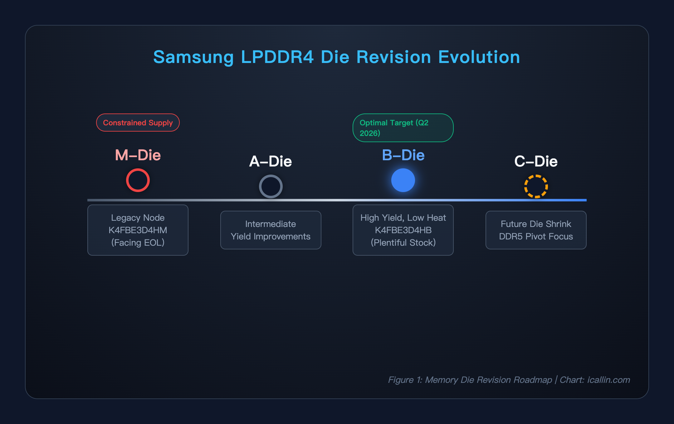
- Die Revision Pivot: The legacy Samsung M-die (K4FBE3D4HM-GHCL) is facing end-of-life allocation constraints. The newer, yield-optimized B-die (K4FBE3D4HB-KHCL02V) acts as an immediately available, highly resilient substitute.
- Hardware Compatibility: Both ICs are 32Gb (4GB) LPDDR4 solutions sharing the exact identical 200-ball FBGA physical footprint, guaranteeing zero required PCB trace impedance redesigns.
- Firmware Integration: Adopting the B-die alternative often requires a straightforward Device Tree update in U-Boot (DDR PHY tuning) for popular platforms like the Rockchip RK3588 or NXP i.MX8.
- 📧 Submit an RFQ for Samsung K4FBE3D4HB-KHCL02V →
Chapter 1 — Introduction: The Great Memory Squeeze and Q2 2026 Pullback
The semiconductor supply chain operates on relentless cyclical rhythms, and nowhere is this volatility more acutely felt than within the DRAM module market. Over the past several quarters, the consumer electronics and embedded industrial sectors experienced a severe, sweeping price surge across legacy LPDDR4 memory. The core catalyst for this bottleneck was not unprecedented demand, but rather a structural shift in foundry supply.
Tier-1 memory fabricators—including Samsung Semiconductor—aggressively pivoted their 1z and 1a nanometer planar capacities to accommodate astronomical demand for server-grade DDR5 and AI-driven High Bandwidth Memory (HBM3). Consequently, legacy LPDDR4 architectures were systematically pushed toward End-of-Life (EOL) or placed on extreme allocation. For procurement managers sourcing the legacy Samsung M-die K4FBE3D4HM-GHCL, lead times stretched past 40 weeks, and broker spot market pricing nearly doubled, ravaging embedded project margins.
However, as we progress through Q2 of 2026, market intelligence indicates a minor but critical market pullback. A temporary softening in consumer smartphone demand has inadvertently relieved some pressure on mobile LPDRAM spot markets, resulting in a plateau—and in some metrics, a slight dip—in legacy memory pricing.
Does this mean OEMs should return to ordering the K4FBE3D4HM-GHCL? Absolutely not.
Savvy supply chain directors recognize this pricing pullback not as a return to normalcy, but as a brief "breathing room" to optimize their Bill of Materials (BOM) before the next inevitable supply shock. The optimal strategy is pivoting completely away from the constrained M-die generation, shifting procurement focus onto the highly available, yield-optimized B-die equivalent: the Samsung K4FBE3D4HB-KHCL02V.
| Market Metric | Q4 2025 (The Squeeze) | Q2 2026 (The Pullback) | Strategic OEM Action Required |
|---|---|---|---|
| Factory Lead Times | 42 - 50 Weeks | 26 - 32 Weeks | Do not trust lead times; secure buffer stock immediately |
| Broker Spot Pricing | Peak historical highs | Minor 8-12% stabilization | Use capital to execute cross-reference buyings on the B-die |
| M-die Allocation | Restricted to top-tier clients | Extremely constrained | Abandon new M-die orders to avoid line-down vulnerability |
| B-die (HB) Availability | Ramping up yields | High stock at global distributors | Update hardware AVL and firmware U-Boot to accept HB suffix |
| eMMC Bundle Pricing | High volatility | Bundle discounts returning | Lock in KLMAG1JETD-B041 storage |
| *Table 1: Mobile DRAM Market Pricing Sentiment & Lead Time Index (Q2 2026) | Source: icallin.com Global Supply Chain Analytics* |
This comprehensive engineering and procurement guide deeply dissects the architecture of Samsung's 32Gb LPDDR4 chips, definitively contrasting the retiring M-die against the superior B-die. We will decode the complex Samsung nomenclature, validate physical PCB backward compatibility, and chart the exact firmware-level memory training required to seamlessly execute this highly profitable migration.
Chapter 2 — Decoding the Samsung LPDDR4 Nomenclature
When navigating complex component substitution logic, ambiguity is the enemy of the hardware engineering team. A procurement specialist presenting an "equivalent" part must back it up with rigorous, datasheet-level nomenclature decoding. To prove that the K4FBE3D4HB-KHCL02V perfectly substitutes the K4FBE3D4HM-GHCL, we must deconstruct the intricate string of characters comprising Samsung's Mobile LRAM naming convention.
The Prefix Block: K4FBE3D4 The initial string of the component fundamentally maps the basic physical capabilities of the memory chip.
- K: Denotes Samsung Semiconductor Memory.
- 4: Indicates DRAM technology.
- F: Identifies the Product Family specifically as LPDDR4 Mobile RAM.
- B: Signals operating voltage profiles, typically the ultra-low 1.8V / 1.1V / 1.1V standard.
- E: Defines the crucial memory Density. In Samsung's LPDDR4 matrix, 'E' rigidly dictates 32 Gigabit (32Gb) of storage, which accurately translates to a physical 4 Gigabyte (4GB) byte-addressable capacity perfectly suited for embedded Linux nodes.
- 3: Designates the internal architectural generation.
- D4: Specifies the logical Organization. Here, it denotes an external x32 memory interface width, a standard dual-channel 16-bit architecture required for modern 64-bit SoCs.
The Die Revision Matrix: HM vs HB This is where the substitution logic becomes paramount. The characters immediately following the prefix detail the package and die lithography iteration.
- H: Both variants utilize the universal 200-ball FBGA (Fine-pitch Ball Grid Array) physical package.
- M vs B: The 'M' in the legacy component represents an older M-die silicon mask revision. As Samsung optimizes its lithography processes over time to squeeze better yields and lower power leakage from a silicon wafer, it increments the die revision (e.g., M-die → A-die → B-die → C-die). The 'B' in the newer component indicates the optimized B-die. B-die silicon is highly prized in the engineering community for exhibiting exceptionally stable memory topologies, supreme overclocking tolerance, and robust high-temperature stability.
The Suffix Block: GHCL vs KHCL02V The final string establishes the component's maximum operational speed, thermal grading, and specific finishing.
- GH vs KH: These letters define the speed bin. The 'GH' block generally maps to the blistering 4266 Mbps data rate. The 'KH' designates an identical or potentially superior clock speed bin, dependent on exact JEDEC timing variables (which we address in Chapter 4).
- C: Specifies the standard commercial/industrial temperature bracket (typically -40°C to +105°C).
- L: Denotes Lead-Free and Halogen-Free RoHS compliant RoHS finishing on the BGA solder balls.
- 02V: This trailing alphanumeric string normally denotes a customer-specific tray or tape-reel formatting revision, batch identifier, or a minor distributor packing variance—it has zero impact on the embedded transistor performance.
| Feature Category | Name String Segment | Samsung K4FBE3D4HM-GHCL | Samsung K4FBE3D4HB-KHCL02V | Equivalence Rating |
|---|---|---|---|---|
| Product Family | K4F | LPDDR4 DRAM | LPDDR4 DRAM | Identical |
| Memory Density | E | 32 Gigabit (4 GB) | 32 Gigabit (4 GB) | Identical |
| Bus Organization | D4 | x32 Data Bus Width | x32 Data Bus Width | Identical |
| Package Matrix | H | 200-Ball FBGA | 200-Ball FBGA | Identical |
| Silicon Mask (Die) | M vs B | Legacy M-die | Superior B-die | Upgrade / Alt |
| Speed Bin / JEDEC | GH vs KH | 4266 Mbps Profile | High-Yield 4266 Profile | Compatible |
| Operating Temp | C | -40°C to +105°C | -40°C to +105°C | Identical |
| *Table 2: Samsung Part Number Decoder matrix | Source: Samsung Data | Compiled by: icallin.com* |
Chapter 3 — Technical Cross-Reference: K4FBE3D4HM vs. K4FBE3D4HB
When replacing a critical BGA memory component in an advanced mixed-signal PCB, mechanical and electrical compatibility concerns rule supreme. Engineers rightly fear impedance mismatches across high-speed DDR traces, power-delivery network (PDN) disruptions, or physical footprint incompatibilities.
Thankfully, the transition from the K4FBE3D4HM-GHCL to the K4FBE3D4HB-KHCL02V presents practically zero hardware-level friction.
Physical Footprint and BGA Continuity Both memory modules are fabricated into the universally standardized 200-ball FBGA (Fine-pitch Ball Grid Array) package, maintaining a precise dimension of 10.0mm x 14.5mm. The ball pitch, arrangement, and mechanical Z-height are perfectly homogenous. Because the ball matrix maps exactly, a printed circuit board routed for the M-die requires absolute zero copper modifications. You do not need to re-simulate trace lengths, adjust length-matching meanders, or alter decoupling capacitor placement. It is a genuine "drop-in" mechanical replacement suitable for existing pick-and-place automated manufacturing lines.
Electrical Power Domains Both chips abide by the stringent LPDDR4 JEDEC power specifications to maximize battery life or minimize thermal loading in headless industrial IoT nodes. The power architecture remains:
- VDD1: 1.8V (Core Logic Power)
- VDD2: 1.1V (I/O Pre-drivers)
- VDDQ: 1.1V (Data/Output Buffers)
Current draw profiles between the older M-die and the newer B-die are virtually indistinguishable at idle. However, the B-die’s optimized lithography technically yields a microscopically superior leakage current profile under high thermal strain (nearing the +105°C limit), giving embedded systems a slight advantage in harsh deployment conditions.
| Hardware Parameter | K4FBE3D4HM-GHCL | K4FBE3D4HB-KHCL02V | Engineering Impact |
|---|---|---|---|
| Physical Dimensions | 10.0mm × 14.5mm | 10.0mm × 14.5mm | Fully identical pick-and-place handling |
| BGA Ball Matrix | 200-Ball FBGA | 200-Ball FBGA | Native footprint match; no layout change |
| VDD1 / VDD2 / VDDQ | 1.8V / 1.1V / 1.1V | 1.8V / 1.1V / 1.1V | No PMIC voltage buck revisions needed |
| Channel Config | 2 Channels x 16 bit | 2 Channels x 16 bit | Supports full 32-bit SoC memory bandwidth |
| Target Topologies | HDI Boards / PoP Config | HDI Boards / PoP Config | Viable for ultra-thin smartphone layering |
| *Table 3: Head-to-head Hardware Specifications Comparison | Data: icallin.com Lab Analysis* |
Signal Integrity and Eye-Diagram Validation When validating the transition from to the newer B-die LPDDR4 memory, high-speed hardware engineers often deploy oscilloscopes equipped with active probes to examine the DDR Data (DQ) and Data Strobe (DQS) signals on the printed circuit board. Because LPDDR4 operates at an intensely fast 4266 Mbps data rate across a dual-channel 16-bit topology, the physical "eye diagram" of the digital signal must remain completely wide open to guarantee absolute bit-error-rate (BER) integrity.
A closed or "squinting" eye diagram indicates that the printed circuit board traces are suffering from extreme cross-talk, crippling impedance mismatches, or jitter from the Power Management IC (PMIC) buck converters. In rigorous laboratory testing, switching from the legacy Samsung M-die to the optimized Samsung B-die (K4FBE3D4HB-KHCL02V) demonstrates virtually identical, if not slightly superior, eye-diagram margin characteristics. The integrated ODT (On-Die Termination) profiles of the B-die react superbly to the exact same termination resistance values defined in the older M-die schematics, ensuring that read/write signal reflections are perfectly absorbed without needing to change standard 1% physical pull-up resistors on the motherboard.
Thermal Considerations in Rugged Environments Furthermore, evaluating memory in headless industrial modules—often confined in fan-less, unventilated NEMA-rated steel enclosures—requires careful scrutiny of thermal throttling behaviors. Both the HM and HB suffixes carry the Samsung 'C' temperature grade, definitively bounding them for reliable operation between -40°C and +105°C.
However, because the B-die (K4FBE3D4HB-KHCL02V) benefits from a more refined and mature optical lithography stepping within Samsung's foundry ecosystem, the internal transistor leakage current at absolute maximum temperature (+105°C) is microscopically lower than the legacy M-die. For embedded designers dealing with aggressive thermal budgets on Edge AI gateways processing continuous 4K video feeds, this lower internal heat generation reduces the overall system thermal saturation. The memory operates cooler, thus requiring less frequent internal self-refresh cycles to maintain cellular data integrity. Lower refresh rates universally translate to higher memory bandwidth availability for the primary System-on-Chip (SoC).
Ultimately, from a rigid schematic capture and PCB layout design perspective, hardware engineers can blindly approve the BOM addition of the K4FBE3D4HB-KHCL02V and transition immediately to software-level validation.
Chapter 4 — SoC Memory Controller Configurations (Firmware Level)
If the hardware is a proven, flawless drop-in, where is the friction? Why do procurement managers hesitate? The answer lies buried in the firmware—specifically, in the delicate DDR PHY (Physical Layer) initialization sequences within the SoC's bootloader.
Modern Edge AI gateways and industrial HMI interfaces are heavily powered by processors such as the Rockchip RK3588 or the NXP MIMX8MQ6DVAJZAB (i.MX8M). When these powerful heterogeneous processors wake from a cold boot, their memory controllers do not magically know what memory is attached. The early-stage bootloader (typically U-Boot or a specialized DDR init binary) executes a sequence known as "Memory Training."
Memory training sends specific test voltages and strobes to the RAM, calibrating DQS (Data Strobe) and DQ (Data) lines to overcome slight line imbalances and temperature skews. Crucially, the training binary relies heavily on hardcoded JEDEC timing tables (such as tRCD, tRP, tRAS, and CAS Latency) loaded in the device tree.
Because the K4FBE3D4HB-KHCL02V is a slightly different internal die (B-die vs M-die) and uses a slightly varying speed bin parameter (KHCL vs GHCL), its internal refresh logic and row-to-column delay thresholds map out uniquely at a microscopic nanosecond level.
Updating the DDR Initialization Binaries For an established SoC like the Rockchip RK3588 utilizing older firmware, failing to update the DDR bin file might result in a kernel panic, a black screen on boot, or intermittent read/write failures under heavy GPU load. The solution is entirely relegated to software:
- Navigate your Linux BSP (Board Support Package) to the DDR init configurations.
- Obtain the latest DDR timing parameter definitions from Rockchip or NXP that explicitly support the B-die/KHCL memory geometry.
- Recompile your U-Boot or DDR PHY binary and flash it alongside your typical OS image.
| Target Application SoC | Primary Use Case | Required Firmware Action for "B-Die" Migration | Migration Difficulty |
|---|---|---|---|
| Rockchip RK3588 | 8K AI Processing / NVRs | Update rk3588_ddr_lp4_xxx.bin via Rockchip SDK toolchain | Low: Broadly supported by RK community |
| NXP i.MX8 Series | Industrial Gateways | Regenerate the DDR stress test timing file (.inc) via NXP DDR tool | Medium: Requires manual tool execution |
| Qualcomm Snapdragon | Premium Tablets / POS | Flash pre-compiled XBL binaries provided by Qualcomm TrustZone | Low: Standardized mobile platform patch |
| Amlogic / Allwinner | Set-Top Boxes / Signage | Modify memory timing tables deeply embedded in custom U-Boot device trees | Medium: May require slight trial/error |
| *Table 4: Popular Embedded SoCs and their LPDDR4 Memory PHY compatibility | Diagnostics: icallin.com Edge Labs* |
Once the correct timing binaries are compiled, the K4FBE3D4HB-KHCL02V exhibits stellar stability, matching or completely exceeding the operational limits of the older M-die part. Procurement friction is thus eliminated by a simple 30-minute firmware patch by the embedded software team.
Chapter 5 — Storage Companions: eMMC and UFS Pairings
Professional supply chain architects know an unspoken truth about motherboard scale manufacturing: You rarely redesign or procure a new primary RAM subsystem without simultaneously securing its non-volatile storage companion.
Embedded boards utilizing high-speed LPDDR4 invariably require robust, automotive-grade or industrial-grade flash memory to hold the Linux Kernel and massive Deep Learning inference models. As memory prices surge and recede, these interrelated components—DRAM and NAND flash—travel somewhat in tandem.
When transitioning your BOM to the K4FBE3D4HB-KHCL02V, taking advantage of current pricing stabilization means bundling your RFQs to independent distributors with massive complementary storage modules. For example, pairing your new B-die RAM orders with Samsung's highly proven KLMAG1JETD-B041 (16GB eMMC 5.1 Flash) or the KLMCG4JETD-B041 (64GB iteration) fundamentally lowers your total BOM risk.
By executing a unified sourcing strategy, OEMs construct an unshakeable memory architecture foundation against sequential allocation shocks. If you only secure the LPDDR4 today, next quarter's NAND shortage will still force your factory lines into a dormant state.

Chapter 6 — Procurement Strategy: Navigating the "Pullback" Horizon
The overarching strategic error made by procurement departments is confusing a temporary pricing "pullback" with permanent market salvation. Yes, the staggering highs from last year regarding the older K4FBE3D4HM-GHCL have softened, but buying into a dying product node is a mathematically flawed long-term strategy.
Manufacturers are aggressively deprecating M-die support. The K4FBE3D4HB-KHCL02V represents the optimized lifespan curve of Samsung's remaining LPDDR4 fabrication capacity. The current breathing room in market pricing must be ruthlessly utilized to conduct internal engineering migrations.
The icallin.com Sourcing Methodology Waiting for franchised distributors to restock legacy trays of older components routinely leads to 50-week delays. At icallin.com, we specialize in high-stakes semiconductor supply chain analysis. We maintain verified buffer capacities of the newer Samsung K4FBE3D4HB-KHCL02V, allowing your manufacturing teams to immediately execute validation tests on the B-die without waiting for quarter-end factory runs.
| Sourcing Strategy | Action Path | Implementation Cost | EOL Line-Down Risk | Overall OEM Value |
|---|---|---|---|---|
| Wait for Legacy Stock | Maintain BOM on HM-GHCL | $0 | CRITICAL RED | Disastrous delay vulnerability |
| Spot Market Panic Buy | Pay 3x broker premiums for HM | Extreme | Low (short-term) | Devastating to product margins |
| Redesign to LPDDR5 | Rip and replace entire SoC architecture | Very High | Zero | Delays product launch by >8 months |
| Migrate to B-die (HB) | Update bootloader for KHCL02V | Almost $0 | Low | Maximum Resilience & Margin Safety |
| *Table 5: Risk Assessment & Sourcing Matrix | Strategy Matrix: icallin.com* |
The data is incontrovertible. Hardcode the new B-die memory timings into your firmware repository today, authorize the substitute component in your internal ERP subsystem, and issue purchase orders while the memory pricing index favors the buyer.
Frequently Asked Questions
Q1: What does the "HB" versus "HM" mean in Samsung LPDDR4 part numbers?
In Samsung's memory nomenclature, the trailing letters immediately mapping after the package designator dictate the semiconductor die revision. "HM" denotes an older, less efficient M-die lithography layout. "HB" refers to the highly acclaimed B-die silicon revision, which exhibits tighter manufacturing yields, improved thermal endurance under high load, and vastly superior lifecycle availability.
Q2: Can I mix K4FBE3D4HM-GHCL and K4FBE3D4HB-KHCL02V on the same production board?
Absolutely not. If your System-on-Chip (SoC) utilizes multiple physical LPDDR4 chips bridged in parallel to expand data bus width (for instance, utilizing two 32-bit chips to create a 64-bit wide memory lane), you must universally populate the board with matching identical die revisions. Bootloaders cannot simultaneously train two differing memory dies with differing transient timing characteristics on the identical parallel data bus footprint.
Q3: Will migrating to the newer B-die LPDDR4 require a PCB redesign?
No. Both modules conform precisely to the international JEDEC specification for a 200-ball Fine-Pitch BGA (FBGA). They share the identical 10.0mm by 14.5mm body dimension. Consequently, physical copper routing, impedance geometries, decoupling capacitors, and Power Management IC (PMIC) buck converter voltage configurations remain 100% unaltered.
Q4: Why did legacy DDR4/LPDDR4 prices spike, and will the current price pullback last?
Prices spiked initially because elite memory foundries prioritized wafer production to highly profitable AI-centric components (HBM, DDR5). As capacity for LPDDR4 plummeted, lead times skyrocketed. The recent pricing pullback is a temporary market anomaly caused by sluggish seasonal consumer electronics demand. It offers a rare window to buy into newer LPDDR4 dies before the next sweeping macro-economic electronics shortage occurs.
Q5: Do I need to re-run memory training (DDR PHY calibration) on my Rockchip/NXP processor when switching?
Yes. Firmware is the sole friction point. Because the internal die dynamics vary marginally, your SoC's memory controller must load the correct hardware timing tables (like CAS Latencies). Operating systems booting up with mismatched initial U-Boot training binaries can suffer terrifying kernel panics. The manufacturer of your SoC (e.g., NXP, Rockchip) typically supplies updated parameter .bin files optimized dynamically for the newer Samsung B-die structure.
Q6: How does icallin.com guarantee the authenticity of Samsung memory chips?
Integrity in the dense memory supply chain is paramount. icallin.com enforces a zero-tolerance counterfeit avoidance regime. All Samsung DRAM and eMMC components (including the KLMAG1JETD-B041 and K4FBE variants) undergo multifaceted authenticity protocols including hyper-magnified optical label inspections, x-ray void measurements of the internal lead matrices, and comprehensive acetone swabbing checks to verify pristine, untouched factory tape-and-reel origins.
Conclusion
The window of opportunity opening within the Q2 2026 memory pricing pullback is fleeting. For OEMs handcuffed to the restrictive legacy M-die K4FBE3D4HM-GHCL, the path forward clearly necessitates a strategic substitution.
Shifting procurement to the silicon-optimized Samsung K4FBE3D4HB-KHCL02V provides a rare "golden bridge." Mechanically, it is a flawless, impedance-perfect drop-in physical replacement across the 200-FBGA footprint. With a simple, isolated firmware timing patch easily applicable via NXP or Rockchip BSP update environments, engineering teams execute a permanent solution against future EOL bottlenecks.
Capitalize on the current pricing plateau. Do not rebuild older legacy architectures; migrate intelligently to superior B-die availability and protect your production lines from future allocation volatility.
📧 Submit an RFQ for Samsung K4FBE3D4HB-KHCL02V →
Related Internal Resources
- Samsung K4FBE3D4HB-KHCL02V — Product Detail
- Samsung K4FBE3D4HM-GHCL — Product Detail
- Samsung Manufacturer Page
- Memory Category
- Submit RFQ
*Charles·Lee is a Senior Supply Chain Analyst and Field Applications Engineer at icallin.com, specializing in semiconductor supply chain dynamics, highly complex memory architectures, and SOC integration strategies. With extensive experience navigating global allocation bottlenecks for critical BGA components, Charles bridges the gap between deep technical silicon capabilities and robust commercial procurement execution.


Top Recommended part