Why So Many Teams Still Use STM32F407ZGT6 in Industrial Control and Embedded Gateways?
When you choose an MCU, the real fear is usually not that the specs look weak. The real fear is finding out halfway through the project that performance is tight, ecosystem support is fragmented, migration is painful, and supply is unstable. STM32F407ZGT6 is an old but famous part. It is still discussed a lot, and it is still debated. Some engineers see it as a classic workhorse. Others think it should be replaced by newer platforms.
I reorganized its core microarchitecture, practical deployment scenarios, mainstream competitors, and the risk points in domestic replacement paths. The conclusion first: it is not a blind default choice, but for projects that value long-term maintenance, mature tooling, and dense peripheral integration, it is still a very stable engineering option.
This article answers three questions. Where does its practical performance ceiling come from? What kinds of real workloads can it carry? Where exactly does it differ from competitors and replacements? If you are selecting parts for a new product or planning second-source migration for an existing one, these are usually the decision-critical points.
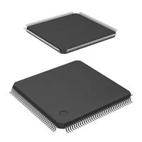
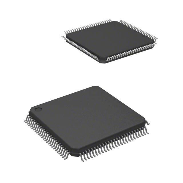
Start with the part number: what STM32F407ZGT6 actually means
The part number itself carries key information:
F4: based on a high performance ARM Cortex-M4 core.07: this sub-family includes Ethernet and full USB OTG.Z: 144-pin package with abundant GPIO resources.G: 1 Mbyte Flash.T: LQFP thin quad flat package.6: industrial temperature range,-40 C to 85 C.
If your project needs control, communication, and a certain amount of signal processing at the same time, this F407 positioning usually fits well.
One easy-to-miss point: the Z package means 144 pins, and that matters a lot at system design stage. It is not only about having more GPIO. It is about reducing pin-mux conflicts. Early versions of a project may use only part of the interfaces, but future feature additions are less likely to force a full PCB redesign. For products that iterate frequently, this expansion headroom is practical value.
The original draft broke down the part number at fine granularity, and that is a good habit for technical selection reviews as well. Check the core, peripherals, package, and temperature grade together before moving into schematic phase. That helps avoid expensive rework later, such as code that runs but an environment that does not fit, or performance that is enough but interfaces that are not.
Microarchitecture in plain terms: why it holds up in real projects
Cortex-M4 + FPU + DSP: the compute base is solid
STM32F407ZGT6 runs up to 168 MHz on a 32-bit Cortex-M4 core. It integrates a single-precision FPU, DSP instructions, and an MPU. Theoretical integer performance is 210 DMIPS (1.25 DMIPS/MHz, Dhrystone 2.1 metric).
What this means in practice is simple: control algorithms, filtering, and protocol stacks can move in parallel, and you do not need to fight daily over whether compute budget is enough.
A point from the original draft is worth keeping: evaluating an MCU by clock frequency alone is incomplete. Frequency is only engine RPM. Whether performance is delivered consistently depends on instruction fetch, data movement, bus contention, and peripheral concurrency. F407 is stable in field projects mostly because of balanced system-level design, not because of one high-frequency label.
The MPU value is also clearer in RTOS projects. With better task isolation, debugging and fault localization costs go down, and behavior remains more controllable when multiple middleware stacks are layered together.
In engineering meetings, 210 DMIPS is often used as a marketing number, but its real value depends on sustained usable performance. After the system enters high load, can it still keep real-time timing? Does bus contention create jitter? Do memory-access bottlenecks disturb control loops? The original draft was strong here because it separated headline compute numbers from deliverable system performance.
ART Accelerator: reducing Flash access bottlenecks
A common high-frequency MCU problem is the memory wall. CPU runs fast, Flash cannot feed instructions quickly enough, and fetch cycles stall. The original draft states that without optimization, wait states can reach 5 cycles or more.
F407 addresses this with ART Accelerator. It includes a 128-bit prefetch queue plus branch prediction and cache mechanisms, enabling what the original document describes as zero-wait-state execution from Flash at 168 MHz. This is a major reason why F407 feels stable in complex firmware.
Put simply: with the same 168 MHz, CPU waits repeatedly for Flash without this mechanism. With ART, fetch efficiency increases and real-time scheduling jitter is easier to control. The original article also linked this to power behavior: less idle waiting by CPU means less dynamic power waste.
This also explains why platforms with the same clock can feel very different as firmware complexity grows. In tiny programs the gap is small. As code size increases, branches increase, and peripheral concurrency rises, fetch and cache policy start to dominate stability. ART is not just a benchmark booster. In real-time systems, it behaves more like a low-level safety fuse.
Memory is not one large SRAM block, but a layered architecture
This chip provides 1 MB Flash + 192 KB SRAM + 4 KB Backup SRAM + 512 Byte OTP. The key point is that 192 KB SRAM is layered, not a single flat block.
| Memory block | Capacity | Connectivity | Practical recommendation |
|---|---|---|---|
| SRAM1 | 112 KB | On AHB bus matrix, accessible by CPU and DMA | Global variables, protocol TX/RX buffers, display frame buffers |
| SRAM2 | 16 KB | Independent physical block, also bus-accessible | Dedicated workspace for selected DMA channels to reduce bus contention |
| CCM RAM | 64 KB | D-bus direct to Cortex-M4, DMA cannot address it | RTOS task stacks, ISR critical variables, pure compute DSP data |
| Backup SRAM | 4 KB | Retained when main VDD is off and VBAT is present | Wake state parameters, critical snapshots, key-like retained data |
The 64 KB CCM is especially important. It avoids direct contention with peripheral DMA and gives CPU more deterministic access. The tradeoff is explicit: linker scripts must be written carefully, and non-DMA critical data must be placed manually.
If you have built systems that run network RX/TX, image capture, and control loops in parallel, this design value is obvious. While Ethernet DMA and camera DMA move data into main SRAM, CPU can still read key control data from CCM smoothly. For motor control or high-frequency interrupt workloads, this isolation can significantly reduce sporadic jitter.
CCM is not a universal buffer, though. Since DMA cannot reach it, putting DMA destination addresses into CCM by mistake can cause direct failures. In practice, teams should formalize this rule in memory-allocation conventions and verify it repeatedly in linker scripts, code review, and unit tests.
Bus and peripheral matrix: not only usable, but concurrent
F407 uses a 32-bit multi-layer AHB bus matrix. I-bus, D-bus, S-bus, general DMA, Ethernet DMA, and USB HS DMA can access different targets concurrently. This is very friendly for real-time systems.
The original draft called this a central nervous system, and that analogy is accurate. Think of CPU, DMA, Ethernet, and USB as traffic flows competing for roads. A single-bus system is a one-lane road where one slowdown drags everything. A multi-layer matrix is multi-lane concurrency with less congestion. For real-time control, that is a direct reason why certain random stalls are less frequent on F407.
From software architecture perspective, this concurrency also affects task decomposition. Protocol, sampling, and control tasks can be split more cleanly by data path, instead of forcing all critical logic into one priority level just to defend timing.
Based on the original draft, peripheral capabilities can be summarized as follows:
3 x 12-bit ADC, single ADC at2.4 MSPS, triple interleaved up to7.2 MSPS.2 x 12-bit DAC.17timers total, including1216-bit and232-bit timers, plus advanced motor-control timers.10/100M Ethernet MACwith IEEE 1588v2 support, MII or RMII.- Dual USB: FS with internal PHY, HS requiring external ULPI PHY.
2 x CAN 2.0B, plusSDIO.FSMCfor SRAM, PSRAM, NOR, NAND, and often parallel LCD 8080/6800 usage.DCMI8 to 14-bit parallel camera interface, up to54 Mbytes/s.
Looking at these together, F407 positioning is clear. It is not built to chase a single compute peak. It is built as a high-versatility control core that combines control, sampling, networking, storage, and HMI interfaces. It may not look extreme at project start, but it usually leaves more usable headroom for mid-to-late feature expansion.
Viewed by product phase, this is even clearer:
- Concept phase: it helps close core function loops quickly.
- Engineering phase: peripheral coverage can reduce external coprocessor count.
- Mass production phase: mature ecosystem keeps maintenance cost more stable.
These stacked benefits explain why F407 remains active in many older but serious product lines.
Typical deployment scenarios: where its strengths are actually useful
Industrial automation and servo control
Industrial servo systems often run FOC and SVPWM and require strict real-time behavior. The combination of F407 FPU, complementary PWM timers, encoder interfaces, and 7.2 MSPS ADC fits current-loop, speed-loop, and position-loop control architectures. Dual CAN and Ethernet also support legacy fieldbus and IIoT backbone integration.
The original draft highlighted a practical point: advanced timers can output multi-channel complementary PWM directly, which is very convenient for three-phase inverter bridge drive. Combined with encoder inputs and high-speed sampling, the chain from sampling to estimation to modulation to drive becomes more coherent. In PLCs, servo drives, and inverters, deterministic timing is often more critical than one-time peak compute.
There is another field reality: on-site maintenance teams are not always firmware experts. If systems are too sensitive to jitter, after-sales cost grows quickly. A platform like F407, with sufficient performance plus mature ecosystem, usually makes issues more diagnosable and maintainable instead of trapping teams in low-level non-reproducible faults.
Portable medical devices and bio-signal processing
Devices such as multi-parameter monitors and portable ECG units often need high-precision sampling and real-time filtering under strict power budgets. F407 ADC plus DSP instructions can run IIR and FIR processing in real time. Sleep, Stop, and Standby modes plus VBAT retention for RTC and backup registers also help battery-life design.
The hard part here is usually not whether signal can be sampled. It is whether noise and baseline drift can be handled cleanly under low power. The workflow in the original draft is practical: AFE conditioning first, then ADC, then local filtering with DSP instructions. Not flashy, but robust and explainable.
Explainability matters a lot in medical electronics. More complex models are not automatically better. Stable reproducibility and long-cycle verification are usually more valuable. The original draft kept that engineering path: sample quality, filter stability, and power management are treated as a package, not as one maximized metric.
Audio and multimedia front-end
F407 provides up to 3 SPI interfaces, with 2 supporting I2S multiplexing. With audio PLL or high-precision external clocking, it can support higher quality audio paths. The examples in the original draft are typical: USB Audio Class driver-free sound card, real-time FFT spectrum display, or DCMI-based image front-end capture for barcode or access-control face capture.
Clock jitter is unavoidable in audio work. The original draft emphasized audio PLL for a reason: time-base stability is handled at chip side, reducing post-processing compensation pressure. For maker products or teaching demos, this hardware mix can produce visible results quickly.
F407 multimedia capability is best described as practical and restrained. It is not a high-end application processor, but for front-end capture, preprocessing, and light HMI interaction, it keeps system complexity in a comfortable range.
Drone and robotics control hub
3 I2C plus 3 SPI is practical for multi-sensor fusion. Attitude estimation can use Kalman or complementary filtering, PID correction can run in millisecond-class loops, and multi-channel PWM can drive BLDC ESC outputs. 168 MHz headroom helps keep end-to-end latency lower in the perception-estimation-control loop.
Drone and robot systems are highly sensitive to sudden jitter in any part of the loop. F407 strength is that both peripheral concurrency and compute are above minimum practical thresholds, so sensor polling, attitude solving, and actuator control can run concurrently. It is not the top compute platform in flight control, but often more balanced in cost and stability.
Boundaries should also be explicit. If system targets include heavier visual perception or large-scale high-level planning, F407 is usually not the final main processor and is better positioned as a real-time control coprocessor. The original draft followed this same scenario boundary.

Competitors and replacements: do not stop at pin compatibility
International comparisons: NXP K64 and TI TM4C
In the original comparison set, NXP K64 and TI TM4C1294/TM4C123 are the most frequent peers.
- NXP K64: common configuration is
120 MHz,1 MB Flash,256 KB SRAM, with widely recognized low-power behavior. Developer feedback often says NXP bus and peripheral design plus documentation are more straightforward at deep driver level. - TI TM4C: also commonly
120 MHz, with strengths in mixed-signal integration and network throughput with TI-RTOS plus NDK stack.
Back to F407, it still has practical advantages: 168 MHz clock ceiling, peripheral breadth including DCMI, and broad dev-board plus community penetration.
The original draft also kept one controversial but useful point: some senior developers believe parts of STM32 family carry legacy design patterns for backward compatibility, making some peripheral behavior feel less intuitive. That does appear in deep driver work. In other words, F407 limitations are not mysterious. They are mostly historical baggage, not absence of core capability.
For technical leads, this kind of architectural legacy is not always negative. It often means longer ecosystem life, clearer migration paths, and more stable compatibility strategy. If teams know where detours exist and encapsulate drivers early, long-term maintenance remains manageable.
Domestic replacements: compatibility boundaries of GD32 and APM32
This is where many teams encounter real migration traps.
GD32F407ZGT6
The text notes that GD32 is very close in package and pins, with one cited difference where VCAP is set as NC on GD32. But internal architecture is not identical. Flash and execution paths differ, with Shadow SRAM execution mapping differences mentioned in the original draft, including a possible 512 KB plus 512 KB topology example.
The result is mixed. Some tight-loop or DSP stress cases may run faster. But Flash algorithms, Boot0 startup behavior, and PLL/RCC configuration details can differ from STM32. Forcing direct STM32CubeMX binaries onto it can cause crashes or ST-LINK recognition issues.
This is the difference between parameter compatibility and system compatibility. Matching pins only means the board can be assembled. Long-term stable firmware still requires item-by-item validation for startup flow, clock tree, flashing algorithm, and debug chain. Skipping this step usually multiplies troubleshooting cost later.
A practical migration validation split:
- Startup layer: Boot0, clock tree, programming tools, debugger recognition.
- Driver layer: peripheral init, DMA behavior, exception interrupts.
- System layer: RTOS preemption, long-run stack stability, fault recovery.
If any layer is not validated, the project should not move to a replaceable mass-production conclusion.
APM32F407ZGT6
APM32 is close to ST at register-map level, and lightweight bare-metal programs can usually run quickly. But once complex RTOS usage is introduced, such as FreeRTOS v10.x plus newer HAL versions like v1.27.x mentioned in the draft, differences in NVIC priority and context switching can surface as HardFault or kernel crash behavior.
So a successful Hello World does not mean the platform can carry industrial-grade software stacks.
For project managers, this is critical. Migration assessment cannot rely on bring-up success rate alone. It must evaluate behavior under heavy load, long-run operation, and injected faults. Once RTOS, multi-priority interrupts, and complex peripheral concurrency are involved, validation must be system-grade.
The original draft described this issue well as a gray-zone integration problem: single modules look correct, but failures appear after composition. The solution is not guesswork. It is version control, layered regression, and reproducible stress testing.
Side-by-side comparison (core metrics from the original draft)
| Dimension | STM32F407ZGT6 | GD32F407ZGT6 | APM32F407ZGT6 |
|---|---|---|---|
| Theoretical max frequency | 168 MHz | 168 MHz (draft mentions internal heterogeneous overclock potential) | 168 MHz |
| Code acceleration mechanism | ART Accelerator | Internal independent SRAM shadowing execution mapping | ST-like cache prefetch structure |
| Physical pin compatibility | Industry baseline model | Pin-to-pin, with VCAP caveat | Claimed drop-in replacement |
| Key migration risk | Seamless official toolchain | Flash algorithm, RCC tuning, startup logic differences | NVIC priority and context-switch differences |
| Market price range | about $2.92 to $8.85, high fluctuation | about $2.89 to $3.50 | usually priced below ST strategy |

Strengths and weaknesses must both be explicit
Strength: the ecosystem moat is genuinely strong
The hardest thing to replicate in F407 is not one isolated spec. It is the STM32Cube ecosystem. CubeMX visual configuration can front-load Pinmux, clock tree, and middleware initialization for FreeRTOS, LwIP, and FatFS, which improves team collaboration and onboarding speed.
This ecosystem value is often underestimated. It is not just convenience. It also means documents, example projects, community answers, third-party tutorials, and board resources align more easily. By year two or year three of product iteration, this long-term gain is often larger than early savings from a slightly cheaper chip.
In financial terms, ecosystem maturity reduces hidden labor cost: debugging time, training time, handover time, and secondary development time. For teams pursuing stable delivery, this is closer to true cost than unit chip price.
Weakness: hardware errata must be treated seriously
The original draft listed four major errata risks:
- In I2S or SPI master receive scenarios, edge delay on SCK can cause loss of the final bit, leading to audio glitches or communication checksum errors.
- Ethernet MAC can deadlock if TxFIFO flush is triggered in a specific timing window after frame transmit, with no workaround, usually requiring watchdog recovery or strict timing avoidance.
- bxCAN time-triggered communication mode is not effectively available as expected in real silicon, limiting deterministic network use that depends on strict time synchronization.
- Near
-40 C, CSI oscillator startup can fail, and official notes indicate no effective workaround.
If your project runs near these boundaries, bypass strategy must be defined at architecture phase.
A good practice is to write these items as design inputs, not as late debug patches. Examples include adding protocol redundancy checks, timeout recovery state machines in network tasks, and batch low-temperature startup validation. This does not make systems perfect, but it moves risk from random field failures to reproducible lab issues.
For high-reliability industries, it is useful to formalize a template:
- Risk trigger conditions.
- Observable symptoms.
- Mitigation strategy.
- Validation method.
- Regression frequency.
This prevents risk knowledge from disappearing when team members change.
Supply chain and lifecycle: realities that engineering cannot ignore
During the 2020 to 2023 global supply shock, STM32F4 series did experience serious shortage, lead times beyond 52 weeks, and abnormal price expansion. Supply-demand conditions have now largely normalized.
The range cited in the source draft is that, in volume procurement, STM32F407ZGT6 price fell back to roughly about $3 to $7.80, depending on quantity and channel. ST also placed this line into a long-term supply program with commitment at least through 2036.
For long-lifecycle sectors such as medical, power grid, and industrial control, this is highly valuable information.
The draft also explained background factors behind that volatility: pandemic shock, AKM factory fire, and foundry capacity tilt caused a chain reaction in delivery systems. The practical lesson is clear: selection should not be based only on current stock. It should include whether the vendor has long-term supply strategy and execution record.
On supply-chain dimension, F407 now looks more like a mature platform after normalization. It may not be the lowest-cost option, but availability and predictability are often more important in most industries. If your product lifecycle is three to five years or longer, this weight should be increased.
Implementation advice: avoid default settings in both hardware and software
Hardware side
Power network and decoupling
- VDD range:
1.8V to 3.6V. - Place
100 nFhigh-frequency decoupling close to each VDD pin. - Place
10 uFlow-ESR tantalum or ceramic at power entry. - For VDDA, use
100 nF + 1 uFparallel decoupling and isolate from digital rail with ferrite bead or LC filter. - Use single-point strategy between VSSA and VSS to reduce ADC noise risk.
These rules look basic, but this is where projects fail most often. Decoupling far from pins, or rough analog-digital ground treatment, can introduce hidden ADC accuracy and stability issues. Board bring-up is not design qualification. Full-load and boundary-condition behavior is the real acceptance gate.
The original draft emphasized power integrity and high-speed impedance control as reliability baseline. In practice, split testing into staged bring-up, long-run stability, and limit-condition tests, so hardware defects are not misattributed to software.
Clock tree and crystal layout
Internal 16 MHz HSI is fine for general computing. For full-speed USB or high-precision Ethernet, external HSE is recommended.
Network designs commonly use 25 MHz HSE. Through PLL it can generate 168 MHz system clock and USB-required 48 MHz, while matching external Ethernet PHY clock needs. Typical CL1 and CL2 range is 5 pF to 25 pF, plus about 10 pF board-level parasitic estimate.
For crystal routing, shorter is better, with continuous nearby ground reference. EMI-resistant layout should be included from first PCB revision. Many random USB disconnect or heavy-network anomalies are ultimately caused by clock and power integrity, not by protocol stack.
If deployment includes industrial sites, noise environments are usually harsher than lab conditions. Clock chain and power filtering should be designed with margin, not only to the point of basic operation.
RMII and USB high-speed routing
With external PHY such as LAN8720A in RMII mode, 50 MHz REF_CLK should follow 50 ohm controlled impedance, and TX or RX lines should be length-matched as much as possible. USB D+ and D- should target 90 ohm differential impedance and follow USB 2.0 high-speed length rules.
For hardware teams, this should become a layout checklist. Put REF_CLK, RMII data lines, and USB differential constraints directly into design rules to reduce uncertainty from experience-only fixes.
On boards that combine high-speed communication and high-precision sampling, routing priority should be agreed early. Place key clocks and differential pairs first, then regular control lines. This lowers respin probability.
Software side
Toolchain
STM32CubeIDE, based on Eclipse plus GCC and GDB, with CubeMX, can graphically complete pin multiplexing, PLL parameters (M/N/P/Q), and LwIP or FreeRTOS initialization generation.
Another benefit of mature toolchains is transferable knowledge. New team members can take over faster without decoding registers from scratch. For teams under long-term maintenance pressure, this significantly reduces staffing risk.
The original draft also noted CubeMX support for automatic PLL parameter derivation and middleware init generation. These capabilities are very useful for getting a system to a runnable baseline quickly. Advanced optimization still needs manual tuning, but the threshold moves from can we do it to how can we do it better.
HAL vs LL selection
- HAL: high development efficiency, good portability, lower migration cost across families.
- LL: closer to registers, shorter execution path, better for microsecond-class control and high-frequency interrupt critical paths.
A practical strategy is hybrid layering: HAL for non-critical modules to keep velocity, LL for bottleneck modules to keep real-time behavior.
This aligns with the original draft: do not treat HAL or LL as ideology. A safer method is to split modules by latency budget and choose tools separately for data plane and control plane. If latency targets are quantifiable, architecture choices become quantifiable too.
Code organization should follow the same logic: separate business layer from hardware abstraction, keep critical paths in dedicated directories, and maintain independent performance regression scripts. This lowers refactor cost later, whether you move across chip families or switch second-source platforms.
Execution checklist for real selection work (structured from source boundaries)
If you want to convert this analysis into project actions directly, use this sequence. It does not add new facts. It only turns the source information into executable checks.
A. Project initiation stage
- Confirm whether the project needs
168 MHzclass Cortex-M4F compute, including FPU and DSP capability. - Confirm whether peripheral mix includes Ethernet, USB, CAN, SDIO, ADC, timers, display, or camera interfaces at the same time.
- Confirm whether pin and package budget requires
144-pinexpansion headroom. - Confirm whether temperature requirements include
-40 C to 85 Cindustrial conditions. - Confirm whether lifecycle targets require long-term supply commitment, cited at least to
2036in the source.
B. Architecture stage
- Treat memory mapping as architecture input, not a late integration patch: place protocol and DMA buffers in SRAM1 or SRAM2, real-time critical data in CCM, and power-loss retention state in Backup SRAM.
- Separate preemptive control tasks from throughput-oriented data tasks to exploit bus-matrix concurrency and reduce interference.
- Define latency and jitter budgets early for mixed scenarios with high-frequency control and heavy communication.
- Identify boundary conditions that may trigger official errata and mark them in requirement documents.
C. Hardware design stage
- Implement power network exactly as recommended:
100 nFnear each VDD,10 uFat power entry, independent VDDA filtering and digital-rail isolation. - Apply single-point strategy for analog and digital ground to reduce ADC noise and crosstalk.
- Raise clock-chain priority: external HSE for USB or Ethernet scenarios, with
25 MHzbaseline common in network designs. - Validate crystal load capacitors using device specs plus parasitic estimation (
5 pF to 25 pFplus about10 pFparasitic). - Enforce RMII and USB routing impedance rules: REF_CLK
50 ohm, USB D+ and D-90 ohmdifferential, with length matching.
D. Firmware development stage
- Use CubeMX and CubeIDE to build a reproducible runnable baseline for clock tree and middleware initialization.
- Set HAL vs LL boundaries by latency budget: HAL for business peripherals, LL for microsecond-level interrupts and tight control loops.
- Put driver init, DMA behavior, interrupt priority, and RTOS scheduling into one integrated test cycle to avoid the pattern where unit tests pass but system crashes.
- Run long-duration stress tests for network, storage, and control concurrency, and evaluate recovery behavior, not only peak throughput.
E. Second-source and migration evaluation stage
- For GD32 and APM32, do not equate pin compatibility with system compatibility.
- Cover startup path, flash algorithm, clock config, debugger accessibility, and RTOS multi-task preemption in migration validation.
- Run gray-scale validation for FreeRTOS plus HAL version combinations, especially NVIC priority and context-switch paths.
- Build a hardware-difference checklist and include it in release gates. If checks fail, do not enter mass-production decision.
F. Mass production and maintenance stage
- Keep errata risks as long-term maintenance items with fixed regression cadence.
- Track both price range and lead-time changes in supply chain to avoid repeated passive replacement cycles.
- Preserve board design rules, clock strategies, and critical driver version records to support cross-team handover.
- Maintain three non-negotiable baselines: performance issues must be locatable, hardware issues must be reproducible, and replacement plans must be verifiable.
The purpose of this checklist is singular: convert classic chip experience into sustainable delivery capability. The real value of F407 is not one successful demo. It is stable maintenance across years of iteration.
Conclusion: when to choose it, and when not to
The true competitiveness of STM32F407ZGT6 is the combination of performance, peripheral coverage, ecosystem maturity, and supply commitment, not one benchmark number. It does have silicon errata and migration boundaries, but these are manageable in engineering practice if constraints are defined clearly at architecture stage.
If you ask whether it is the most advanced Cortex-M4 solution today, that is not the key question. What matters is that risk boundaries are clear, tooling is mature, community experience is deep, and supply behavior is predictable. For most projects that must launch on time and be maintained long-term, this is more valuable than chasing newer headline parameters.
In engineering, the most reliable selection is usually not the most impressive one. It is the one that is verifiable, maintainable, and deliverable. STM32F407ZGT6 still fits those three words. If you encode known weaknesses into design constraints and layer key modules by real-time budget, it remains a main controller you can ship with confidence.
Suitable for:
- Industrial, medical, and energy projects that require long-term maintenance and stable delivery.
- Systems that need control, communication, and signal processing at once, with high peripheral concurrency pressure.
- Teams that want to rely on mature toolchains and community assets to reduce delivery risk.
Not suitable for:
- Projects with hard dependency on deterministic time-triggered CAN behavior.
- Devices that run for long periods in extreme cold boundaries and depend on CSI startup stability.
- Teams that plan to migrate complex STM32 software stacks to domestic-compatible chips with zero validation.
One-line closing statement: this chip is not new, but it is still practical in many serious projects. The key is not whether it is strong in abstract. The key is whether your system is designed around its real boundary conditions.
Reference links


Top Recommended part