Part No:
EP1S25F672I7N
Category:
Interface ICs
Description:
1.5 V V 237.4 kB B FPGAs Stratix® Series 420.17 MHz MHz 672-BBGA 90 mA mA 1 mm mm
Package:
-
Datasheet:
-
Production Status:
In Stock Status:
Specification
Schedule B
8542390000, 8542390000/8542390000/8542390000/8542390000/8542390000
Moisture Sensitivity Level
Reflow Temperature-Max (s)
Max Operating Temperature
Min Operating Temperature
Peak Reflow Temperature (Cel)
Programmable Logic Type
FIELD PROGRAMMABLE GATE ARRAY
Number of Logic Elements/Cells
Number of Logic Blocks (LABs)
Products Detail
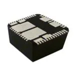
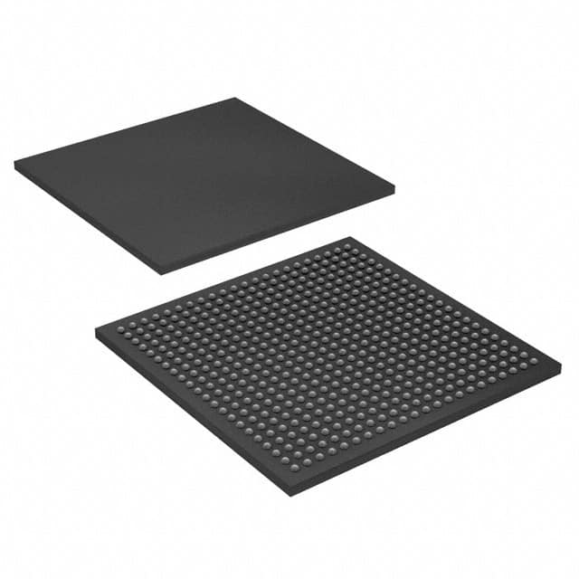
EP1S25F672I7N Overview
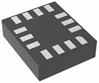
There are two packages that contain fpga chips: 672-BBGA package and X package. The FIELD PROGRAMMABLE GATE ARRAY-series of FPGAs are composed of this type. Having 473 I/Os makes data transfers more coherent. Logic blocks consist of 25660 logic elements/cells. In this case, the FPGA part belongs to the Field Programmable Gate Arrays family. An attachment Surface Mount allows the FPGA module to be attached to the development board. The supply voltage of the device is 1.425 V ~ 1.575 V , at which it runs. The Stratix® series FPGA is a type of FPGA that belongs to the Stratix® family of FPGAs. When operating the machine, it is important to keep the temperature within -40°C ~ 100°C (TJ) range. This device is equipped with 706 separate outputs, which makes it a very versatile device. There is an FPGA model contained in Bulk in order to conserve space. A device like this one offers 1944576 RAM bits, which is a considerable amount of memory. In order to find related parts, use the part number EP1S25 as a base. This FPGA module has a RAM si237.4 kBe of 237.4 kB that is sufficient to make sure that the program is able to run normally. In this case, there are 672 pins on the board. A total of 2566 LABs/CLBs make up this FPGA array. Having stated that, if this FPGA is mounted in Surface Mount, then it may be able to perform fantastically according to its specifications. The 1.5 V supply voltage provides designers with full flexibility in their designs. The device runs on a 1.5,1.5/3.3 V battery and requires no additional power supply to operate. During its maximal operating temperature, this module reaches 100 °C. In order to achieve -40 °C, the operating temperature must be higher than -40 °C. This device has a pin count of 672 in fpga semiconductor. Fpga semiconductor consists of 2566 logic blocks (LABs). Data and programs can be stored in this FPGA module's 237.4 kB memory. Powered by a 420.17 MHz-frequency motor, it delivers high efficiency. A maximum supply voltage of 1.575 V can be applied to this product. The minimal supply voltage required for it is 1.425 V. As far as the speed of this FPGA is concerned, it can get up to 66 MHz. For the building block, it encompasses 25660 logic cells that make up the logic circuit. Fpga semiconductor operates on a 90 mA power supply. The device package supplied by 672-FBGA (27x27) is one of its suppliers. This system's configuration is carried out using 672 terminals.
EP1S25F672I7N Features
473 I/Os
Up to 1944576 RAM bits
672 LABs/CLBs
100 °C gates
2566 logic blocks (LABs)
Operating from a frequency of 420.17 MHz
EP1S25F672I7N Applications
There are a lot of ALTERA
EP1S25F672I7N FPGAs applications.
- Computer hardware emulation
- Integrating multiple SPLDs
- Voice recognition
- Cryptography
- Filtering and communication encoding
- Aerospace and Defense
- Medical Electronics
- Audio
- Automotive
- Consumer Electronics
Key Features
No key features available
Application scenarios
No application scenarios available
Documents