Part No:
STB13NM50N
Category:
Transistors
Description:
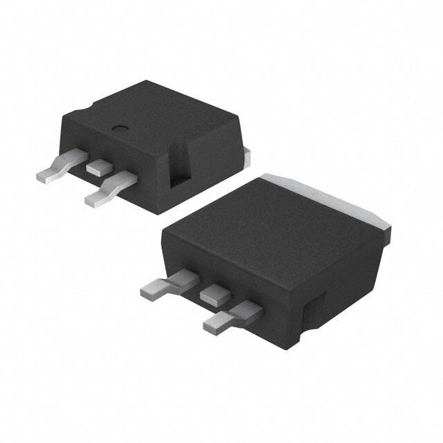
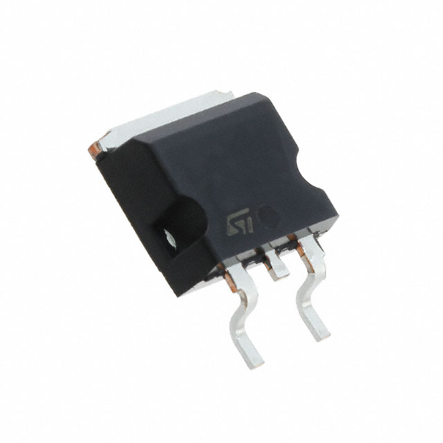
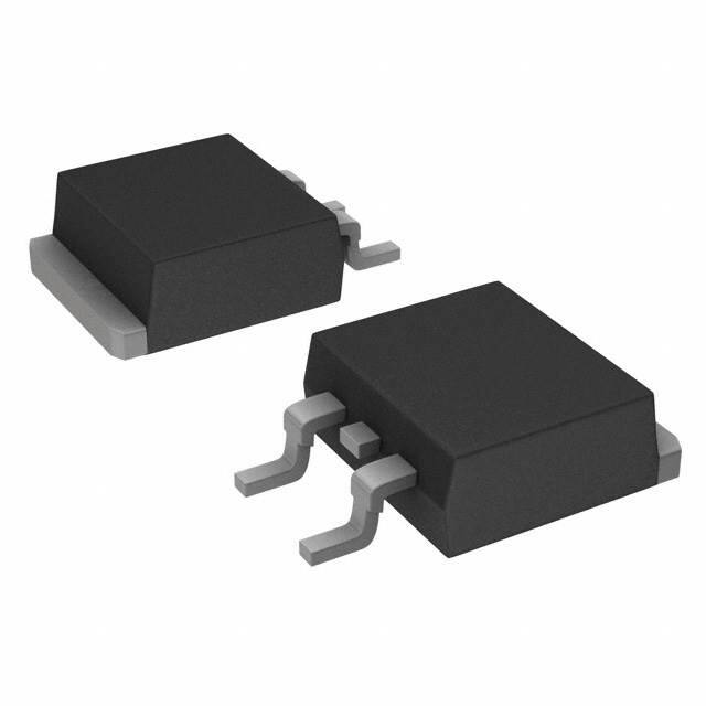
MOSFET (Metal Oxide) N-Channel Tape & Reel (TR) 320m ? @ 6A, 10V ±25V 960pF @ 50V 30nC @ 10V TO-263-3, D2Pak (2 Leads + Tab), TO-263AB
Package:
-
Production Status:
In Stock Status:
Specification
Package / Case
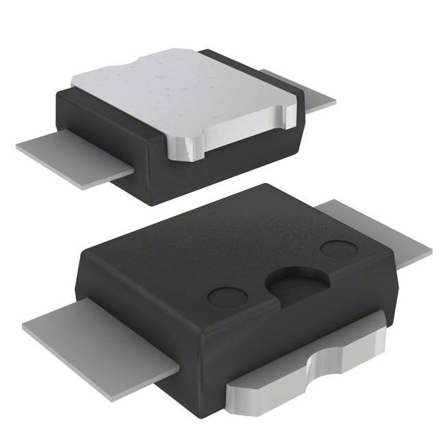
TO-263-3, D2Pak (2 Leads + Tab), TO-263AB
Transistor Element Material
Moisture Sensitivity Level (MSL)
Peak Reflow Temperature (Cel)
Time@Peak Reflow Temperature-Max (s)
Input Capacitance (Ciss) (Max) @ Vds
Current - Continuous Drain (Id) @ 25°C
Gate Charge (Qg) (Max) @ Vgs
Drive Voltage (Max Rds On,Min Rds On)
Continuous Drain Current (ID)
Gate to Source Voltage (Vgs)
Drain to Source Breakdown Voltage
Pulsed Drain Current-Max (IDM)
Avalanche Energy Rating (Eas)
Products Detail
STB13NM50N Overview
When a voltage exceeds breakdown voltage of a MOSFET, breakdown phenomena occurs and current flows. It's called ?Avalanche break down?, and the energy applied to the MOSFET is called avalanche energy, and the avalanche energy rating (Eas) is 200 mJ.The input capacitance parameter, CI, is defined as the capacitance between the input terminals of an op amp with either input grounded, and this device's maximal input capacitance is 960pF @ 50V.The drain current is the maximum continuous current the device can conduct, and the continuous drain current (ID) of this device is 12A. Drain-source breakdown voltage is the VDS at which a specified value of ID flows, with VGS=500V. And this device has 500V drain to source breakdown voltage.Turn-Off delay time is the time taken to charge the input capacitance of the device before drain current conduction can start, and its turn-off delay time is 40 ns.IDM is the maximum rated peak drain current for a power MOSFET, and its maximal pulsed drain current is 48A.Turn-on delay time is the time taken to charge the input capacitance of the device before drain current conduction can start, and its delay time is 30 ns.The gate-source voltage, VGS, of a FET transistor is the voltage that falls across the gate-source terminal of the transistor and its voltage can be 25V.By using drive voltage (10V), this device helps reduce its overall power consumption.
STB13NM50N Features
the avalanche energy rating (Eas) is 200 mJ
a continuous drain current (ID) of 12A
a drain-to-source breakdown voltage of 500V voltage
the turn-off delay time is 40 ns
based on its rated peak drain current 48A.
STB13NM50N Applications
There are a lot of STMicroelectronics
STB13NM50N applications of single MOSFETs transistors.
- LCD/LED TV
- Consumer Appliances
- Lighting
- Uninterruptible Power Supply
- AC-DC Power Supply
- Synchronous Rectification for ATX 1 Server I Telecom PSU
- Motor drives and Uninterruptible Power Supplies
- Micro Solar Inverter
- DC/DC converters
- Power Tools
Key Features
No key features available
Application scenarios
No application scenarios available
Documents