Part No:
STB50N25M5
Category:
Transistors
Description:
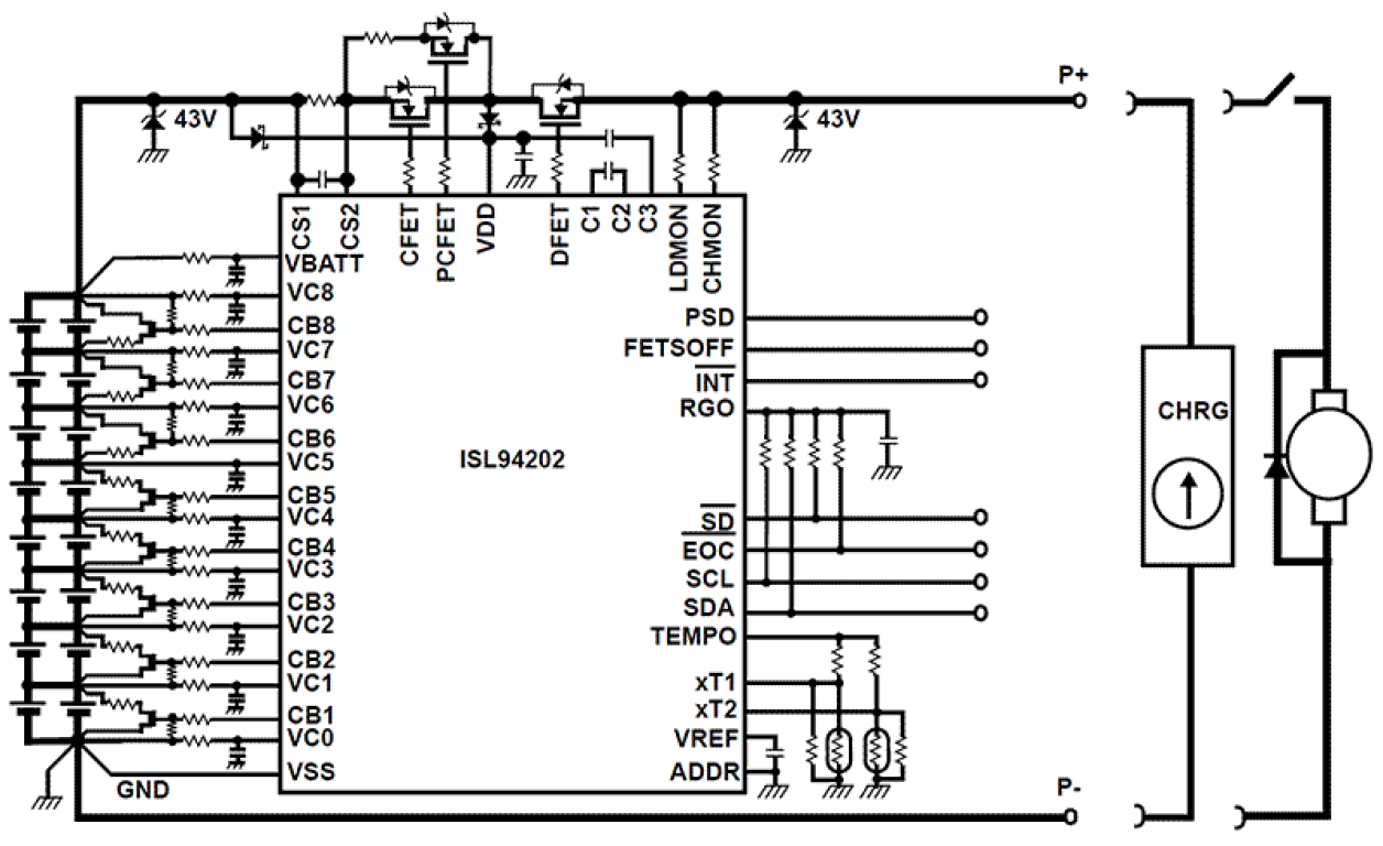
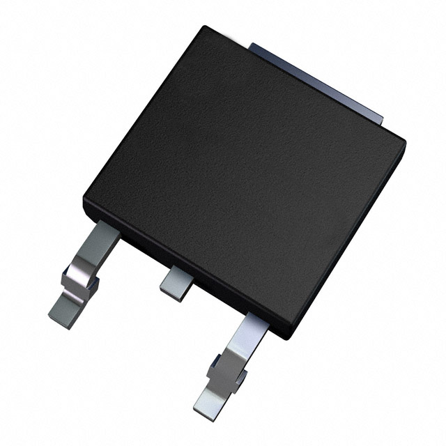
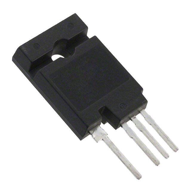
MOSFET (Metal Oxide) N-Channel Tape & Reel (TR) 65m ? @ 14A, 10V ±25V 1700pF @ 50V 44nC @ 10V TO-263-3, D2Pak (2 Leads + Tab), TO-263AB
Package:
-
Production Status:
In Stock Status:
Specification
Package / Case
TO-263-3, D2Pak (2 Leads + Tab), TO-263AB
Transistor Element Material
Moisture Sensitivity Level (MSL)
Terminal Finish
Matte Tin (Sn) - annealed
Peak Reflow Temperature (Cel)
Time@Peak Reflow Temperature-Max (s)
Configuration
SINGLE WITH BUILT-IN DIODE
Input Capacitance (Ciss) (Max) @ Vds
Current - Continuous Drain (Id) @ 25°C
Gate Charge (Qg) (Max) @ Vgs
Drive Voltage (Max Rds On,Min Rds On)
Continuous Drain Current (ID)
Gate to Source Voltage (Vgs)
Drain Current-Max (Abs) (ID)
Drain to Source Breakdown Voltage
Products Detail
STB50N25M5 Overview
An op amp's input capacitance is defined as the capacitance between both of its input terminals with either input grounded, and 1700pF @ 50V is its maximum input capacitance.The drain current is the maximum continuous current the device can conduct, and this device has 14A continuous drain current (ID).A drainage-to-source breakdown voltage corresponds to the voltage at which a specified value of ID flows, where VGS is 250V, and this device has a drainage-to-source breakdown voltage of 250VV.Drain current refers to the maximum continuous current a device can conduct, and it is 28A.Input capacitance must be charged before drain current conduction can begin, so the turn-off delay time is 35 ns.Before drain current conduction begins, the device's input capacitance must be charged, so the delay time is 16 ns.An FET transistor's gate-source voltage, VGS, indicates how much voltage is applied across the transistor's gate-source terminal and it can range from 25V to 1.In this case, the threshold voltage of the transistor is 4V, which means that it will not activate any of its functions when its threshold voltage reaches 4V.Using drive voltage (10V), this device contributes to a reduction in overall power consumption.
STB50N25M5 Features
a continuous drain current (ID) of 14A
a drain-to-source breakdown voltage of 250V voltage
the turn-off delay time is 35 ns
a threshold voltage of 4V
STB50N25M5 Applications
There are a lot of STMicroelectronics
STB50N25M5 applications of single MOSFETs transistors.
- AC-DC Power Supply
- Synchronous Rectification for ATX 1 Server I Telecom PSU
- Motor drives and Uninterruptible Power Supplies
- Micro Solar Inverter
- DC/DC converters
- Power Tools
- Motor Drives and Uninterruptible Power Supples
- Synchronous Rectification
- Battery Protection Circuit
- Telecom 1 Sever Power Supplies
Key Features
No key features available
Application scenarios
No application scenarios available
Documents