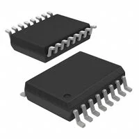
TMS320F2812PGFA: Plan a Fixed-Point C2000 Migration
Author: Charles·Lee | Category: Cross-Reference & Alternatives | Primary part: TMS320F2812PGFA | Manufacturer: Texas Instruments | Updated: 2026-09-10
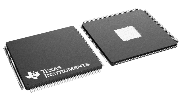
TMS320F2812PGFA is a Texas Instruments C28x fixed-point controller for demanding real-time control tasks. The 176-pin LQFP device offers a 150MHz operating point, 256KB of flash and two Event Managers for motor-control peripherals. Moving an existing design to another C2000 device requires more than matching clock speed: arithmetic scaling, peripheral behavior, memory mapping, package connections and startup timing must be checked together.
Catalog / Key Takeaways
A useful F2812 migration preserves observable behavior before it changes architecture. First establish what the existing controller does at its numeric, timing and electrical boundaries; then decide which differences the new design is allowed to introduce.
- The exact PGFA package and temperature suffix matter independently of the F2812 family name.
- The documented 150 MHz operating point requires a nominal 1.9 V core supply. A nominal 1.8 V operating point is limited to 135 MHz.
- Fixed-point range, rounding and saturation deserve explicit acceptance vectors. Compiling successfully is not equivalent to matching the old controller.
- Event Manager behavior must be translated into the target architecture. F2812 register settings are not an ePWM configuration recipe.
- A related C2000 device is a comparison candidate until the board, software and real-time behavior have been qualified.
Jump to the baseline, voltage and clock check, numeric and memory acceptance, peripheral migration, related devices, or frequently asked questions.
What Must Be Preserved from the F2812 Baseline?
Preserve the requirements implemented by the old design, not every historical implementation detail. A migration can change the controller, compiler and board while retaining the required control behavior, but only if those requirements are written down independently of the old source code.
For TMS320F2812PGFA, start with TI's SPRS174V datasheet, revised February 2021, and the exact ordering entry in its July 15, 2026 package addendum. The supplied document places the PGFA device in a 176-pin LQFP with an ambient range of −40°C to +85°C. The broader family document also discusses other packages and temperature options; those alternatives do not redefine the installed part. TI exact-part documentation, Table 6-1 and ordering addendum.
| Baseline item | Verified value | Applicability | What the migration must establish |
|---|---|---|---|
| Exact device | TMS320F2812PGFA | TI Catalog ordering option | Match the installed bill of materials and package marking |
| Package | PGF, 176-pin LQFP | Exact PGFA order | Reconcile every used signal with the proposed target pinout |
| Ambient range | −40°C to +85°C | PGFA suffix | Confirm the actual board environment and target grade |
| Flash | 128K × 16; 256 KB | F2812 device, binary capacity convention | Compare usable sections, boot allocation and programming method |
| SARAM | 18K × 16; 36 KB | F2812 device | Account for stack, variables, buffers and RAM-resident routines |
| Control peripherals | Two Event Managers | F281x architecture | Preserve the required PWM, capture and event behavior |
| External interface | Present on F2812 | Not a general F281x guarantee | Identify external memory and peripheral dependencies |
Table 1: TMS320F2812PGFA identity and migration baseline | Source: TI SPRS174V, pp1, 5 and ordering addendum | Compiled by: icallin.com
Collect a reproducible baseline before changing the build. Useful artifacts include the released source revision, compiler version and options, linker command file, generated map, programming procedure and board revision. Add the configured clocks, interrupt priorities, ADC sequence, PWM update rules and fault behavior. These are not administrative extras: without them, a changed output may be impossible to attribute to arithmetic, placement, timing or hardware.
Separate three kinds of requirement. A functional requirement describes what the controller should calculate. A temporal requirement specifies when an input is captured and when its resulting output must take effect. An electrical requirement defines valid rails, signal levels and pin behavior. “The motor runs” is too broad to distinguish these categories. It may conceal a shifted sampling point, an occasional missed update or a startup state that was never exercised during a short demonstration.
An existing design also contains accidental behavior. A rounding bias may have been compensated elsewhere; an unused output may happen to be pulled safely by the old board. Decide whether each observation is required, harmless or a defect to be removed. Record intentional changes explicitly so that the qualification team does not mistake an approved correction for a regression.
For a practical handoff, attach expected outputs to a small collection of input records. Include ordinary operating points, transitions between modes, a reset during an unfinished transaction and a fault followed by recovery. Where the old implementation is the reference, state that explicitly; where a written requirement supersedes it, identify that requirement. This prevents an automated comparison from rewarding an inherited defect merely because both controllers reproduce it. Keep the raw input, expected result, allowed tolerance and required observation time together so that another engineer can repeat the test without reconstructing the original assumptions.
The C2000 solar-inverter discussion offers adjacent application context for control workloads. For this migration, however, use the current TI documents for memory, package and timing values. An older application article is not a substitute for the exact-device baseline.
Check Core Voltage Before Comparing Clock Speed
Compare the clock and supply as a supported operating point, not as two independent headline values. TI documents different maximum system clocks for nominal 1.8 V and 1.9 V core supplies, while the I/O range remains the same in the relevant table.
| Nominal core supply | Allowed core range | Maximum SYSCLKOUT | I/O supply range | Interpretation |
|---|---|---|---|---|
| 1.8 V | 1.71–1.89 V | 135 MHz | 3.14–3.47 V | Use this complete operating-point definition |
| 1.9 V | 1.81–2.00 V | 150 MHz | 3.14–3.47 V | Do not assume an existing 1.8 V rail supports the faster point |
Table 2: Documented F2812 core-voltage and system-clock combinations | Source: TI SPRS174V, p21, Recommended Operating Conditions | Compiled by: icallin.com
The overlap between the two voltage ranges does not justify interpolating a new speed grade or treating any nominal supply as adequate. A nominal rail identifies a tolerance budget, and the voltage reaching the package can differ from the regulator's nominal setting. Start with the complete selected operating point, then assess regulator tolerance, distribution drop and transient behavior against its limits.
Consider an illustrative rail review, not a measured board. Suppose a design specifies 1.8 V with ±3% initial regulation accuracy. Its calculated regulator range is 1.746–1.854 V before adding distribution and transient effects. The low end is below the 1.81 V minimum in the 150 MHz row. A typical bench reading near 1.82 V would therefore not establish that the design supports 150 MHz across its defined conditions. The calculation identifies a qualification failure in the proposed tolerance budget; it does not diagnose a particular customer unit.
The same review should include startup and reset, rather than checking only the settled rail. Power sequencing, oscillator startup, PLL configuration, watchdog servicing and peripheral enable order can change the first active output. Consult the device's power-sequencing and clock-control requirements when translating the board design. Do not “fix” a timing problem by increasing a clock until the electrical and flash-access conditions have been checked.
Treat 135 MHz at a nominal 1.8 V core and 150 MHz at a nominal 1.9 V core as two distinct operating points. Each requires its own allowed core-voltage range, while both share the 3.14–3.47 V I/O range. These limits do not establish a continuous voltage-to-frequency relationship: an intermediate supply voltage is not permission to interpolate a new maximum clock, efficiency estimate or performance result.

Clock speed also changes the meaning of a cycle-based budget. As a deliberately simplified example, 1,350 processor cycles occupy 10 µs at 135 MHz and 9 µs at 150 MHz. This conversion says nothing about whether the same routine uses 1,350 cycles after recompilation, whether instruction fetches stall, or whether an interrupt is delayed. It is a bookkeeping tool: measure execution on the actual build, then convert with the actual clock.
Preserve Fixed-Point Arithmetic and the Memory Map
Treat numeric behavior and memory placement as separate acceptance gates. A new implementation can produce the right answer in a desktop calculation and still miss the update deadline, while a fast implementation can apply an incorrect scale or overflow rule consistently.
The F2812 is a fixed-point C28x device; its documentation does not identify the hardware floating-point unit found in the F28335 comparison device. That distinction does not prohibit software floating-point operations, but it does mean that changing arithmetic representation can alter execution time, numerical behavior and toolchain requirements. Keep the initial migration objective narrow: establish equivalent behavior before claiming an algorithmic improvement. TI F2812 documentation, Features and CPU description.
Build numerical tests around boundaries
Define each signal's physical unit, stored representation and valid range. For an illustrative signed fractional format with a scale of 32,768 counts per unit, a stored value of 16,384 represents 0.5. The largest positive 16-bit stored value, 32,767, represents approximately 0.9999695 rather than exactly 1.0. This is a property of the deliberately chosen representation, not a mandatory format imposed by the F2812.
Now multiply two represented values of 0.75. Each input is 24,576 counts; their integer product is 603,979,776. Restoring the original scale gives 18,432 counts, or 0.5625. The intermediate requires more storage than either input. A migration test should therefore verify the operand conversion, intermediate width, scaling operation and destination behavior separately. Matching only the final variable type does not prove the intermediate calculation survived unchanged.
Next test a value that falls between representable outputs. Rounding toward zero, rounding to nearest and an implementation-specific shift of a negative intermediate can produce different least-significant results. Include both signs and specify the required rule in the acceptance record. Do not rely on how an expression happens to behave under one compiler optimization level; consult the selected compiler's documented integer behavior and test the released build.
Finally exercise the limit path. If a hypothetical normalized command calculation requests 1.1, the design must define whether to clamp, flag, rescale or reject it. Wrapping into a negative output is a different behavior from saturation, even if ordinary operating points agree. Test the boundary just below the limit, at the limit and just beyond it. Add a sequence that stays saturated and then returns to the valid range, because stateful control code can retain an internal error after the output has been clamped.
| Design artifact | F2812 baseline to capture | Target evidence required | Proposed acceptance check | Unresolved without project data |
|---|---|---|---|---|
| Signal representation | Units, scale and signed range | Explicit representation and conversion rules | Zero, extrema and values on both sides of a rounding boundary | Required numeric tolerance |
| Multiplication and accumulation | Operand and intermediate widths | Compiler behavior and overflow treatment | Reproduce the 0.75 × 0.75 example, then exercise limits | Actual algorithm's worst intermediate |
| Limit handling | Clamp, wrap, fault or rescale policy | Equivalent or intentionally revised policy | Enter saturation, hold it and recover | Control-state recovery requirement |
| Flash layout | 128K × 16 physical capacity; released map | Section allocation, boot area and programming arrangement | Compare section addresses and placement constraints | Application size and reserved regions |
| SARAM use | 18K × 16 physical capacity; stack and buffers | Peak simultaneous allocation and execution placement | Stress stack and buffer occupancy on the released build | Measured worst-case usage |
| Time-critical routines | Actual memory location and build options | Target placement and measured duration | Check deadlines with representative interrupt interference | Application-specific timing margin |
Table 3: Numerical and memory acceptance evidence for a fixed-point migration | Source: TI SPRS174V, Table 6-1 and CPU/memory descriptions; original qualification procedure | Compiled by: icallin.com
Compare addressable capacity and usable placement
The memory arithmetic is straightforward but easy to mislabel. TI's 128K × 16 flash organization corresponds to 128 × 1,024 × 2 = 262,144 bytes, conventionally listed as 256 KB. The 18K × 16 SARAM organization corresponds to 36,864 bytes, or 36 KB. A word count from the datasheet must not be compared directly with a byte count from another architecture's marketing table.
Usable placement is a different question from total capacity. A boot area, constants, interrupt vectors, stack and RAM-executed routines compete for specific regions. Compare the map, not only the total image size. Check whether external memory is used and whether a target's interface can reproduce the necessary access behavior. A related device without the F2812 external interface may require a board and memory-architecture redesign even when its internal flash is large enough.
TI describes configurable flash wait states and a pipeline option whose performance benefit depends on the application. Consequently, changing where code executes can change deadline behavior without changing source-level calculations. Revalidate startup copying, section alignment, access timing and flash-programming arrangements against the chosen device. The appropriate deliverable is a new verified map and timing record, not a statement that “the binary fits.” SPRS174V memory descriptions, Section 9.1.
The STM32F405RGT6 comparison article can be read as adjacent controller-selection context. Its model relationships do not establish a C2000 substitute. Carry the same discipline into this project: architecture familiarity, source similarity and package resemblance answer different questions from electrical or software compatibility.
Translate Event Manager Behavior into the Target Design
Translate the required event sequence, not the names of old registers. F2812 uses EVA and EVB Event Managers; a target built around ePWM peripherals must be configured from its own documentation to reproduce the intended waveform, sampling, update and protection behavior.
Write the control cycle as a sequence of observable events: time-base position, output transition, sampling trigger, acquisition interval, conversion completion, interrupt service, command calculation and output-register update. Then identify the next event at which that command becomes effective. Two implementations can execute the same arithmetic at the same nominal rate yet differ by an entire update opportunity because their transfer or interrupt rules are different.
The ADC is a useful example of why a single number is inadequate. TI specifies an acquisition width of (1 + Acqps) ADC clock periods for the F281x ADC. At a 25 MHz ADC clock, one period is 40 ns, so settings 0 and 15 correspond to acquisition widths of 40 ns and 640 ns. Those values describe the acquisition window; they are not the entire delay from an external event to usable software data. Preserve the trigger, aperture and result-availability distinctions when reviewing the target. SPRS174V, pp73–74.
| Function | Legacy evidence to capture | Target requirement to establish | Failure boundary |
|---|---|---|---|
| PWM generation | Time base, polarity and output mapping | Same intended switching sequence under the chosen target settings | Matching frequency alone misses polarity or phase changes |
| Command update | When software writes and when hardware applies the value | Defined update opportunity and worst-case deadline | A late write can affect a later cycle |
| ADC acquisition | Clock, Acqps and source-driving arrangement | Valid acquisition interval at the actual ADC clock | A copied register number need not mean the same interval |
| Conversion and interrupt | Trigger-to-result path and interrupt ordering | Data readiness before use and bounded service latency | Acquisition width is mistaken for complete latency |
| Fault handling | Fault source, route, output state and recovery policy | Equivalent required protective behavior | A normal-loop test never exercises the fault route |
| Reset and startup | GPIO and peripheral states before control starts | Defined board-safe initialization sequence | The new output becomes active before configuration is complete |
Table 4: Behavior-based Event Manager migration checks | Source: TI SPRS174V, Features and ADC timing pp73–74; original qualification framework | Compiled by: icallin.com
For a reproducible timing exercise, assume a hypothetical control task has a 50 µs period and a command must be ready within 20 µs of the selected sampling event. These are project assumptions, not F2812 specifications. Allocate the 20 µs across sample/result availability, interrupt-entry delay, calculation and the final write. If a proposed measurement shows 2 µs before usable data, 3 µs of worst-case service delay and 12 µs of calculation plus write, the total is 17 µs and the arithmetic margin is 3 µs. Until those durations are measured on the actual configuration, the example remains a worksheet, not a passed design.
The acceptance test must also establish that its measured worst case is relevant. Exercise concurrent interrupts, maximum buffer activity and the code paths that perform limit handling. Capture the output-update boundary rather than stopping the timer when the calculation returns. Repeat after changing optimization or memory placement. A timing number without the build and interrupt conditions is difficult to reuse during the next release.
Also define what happens when the deadline is missed. A design may retain the previous command, reject a stale result or enter a controlled fault state, but the correct choice comes from its system requirements. Test the selected policy with a deliberately delayed calculation in a controlled setup before exposing a power stage to it. The objective is not to create a dramatic failure demonstration; it is to show that the controller's exceptional path remains understandable when normal scheduling assumptions no longer hold.
Migration acceptance links five areas: arithmetic behavior, compiler/linker output, peripheral-event behavior, board pinout/power and acceptance measurements. These checks are interdependent rather than a sequence performed once. A failed board-level check can require revisiting peripheral mapping; a failed timing check can require revisiting code placement. Keep the affected evidence together when reopening a decision, so a local correction does not silently invalidate a previously accepted result elsewhere.

An EtherCAT motor-control architecture discussion is relevant when communications and control compete for processor time. It is adjacent reading, not evidence that the XMC device can replace this C2000. The useful migration question is which work must stay deterministic and which work may be scheduled around it.
Compare Related C2000 Devices Without a Drop-In Claim
Use related devices to narrow the review, not to skip it. The following matrix distinguishes a same-family option, a temperature variant and architectural comparison candidates. None has been qualified here as a complete board-and-software replacement.
| Model | Relationship | Relevant difference | Required compatibility work |
|---|---|---|---|
| TMS320F2812PGFA | Primary baseline | Fixed-point F2812, 176-pin PGF | Record the released design's actual requirements |
| TMS320F2811PBKA | Related family member | 128-pin package; no F2812 external memory interface | Redesign pin mapping and any external-interface dependency |
| TMS320F2812PGFS | Related family member; unlinked technical reference | Same F2812 architecture; −40°C to +125°C ordering option | Verify exact ordering and board/application qualification |
| TMS320F28335PGFA | Comparison candidate | Hardware FPU and ePWM architecture | Requalify arithmetic, peripherals, pinout and software |
| TMS320F28235PGFA | Comparison candidate | Fixed-point F2823x device with ePWM | Check the complete target architecture and board requirements |
Table 5: Related C2000 devices and the work required before migration | Source: TI F2812 documentation and TI F28335/F2823x documentation | Compiled by: icallin.com
A change to a wider temperature option is not the same project as a change to an FPU-equipped device. The first starts with exact ordering and application qualification; the second introduces a broader architectural review. Likewise, a matching 176-pin count does not prove that two packages have interchangeable signal assignments. Place the actual pin lists side by side before committing a schematic.
For a broader architecture search, the STM32H743 controller overview is contextual reading only. A Cortex-M7 controller is not a drop-in F2812 replacement. Any cross-architecture redesign needs its own peripheral, software, timing and board-level plan, and the older article's commercial headline should not be read as a current availability statement.
Frequently Asked Questions
Is TMS320F2812PGFA a floating-point MCU?
It is a C28x fixed-point control device; the supplied F2812 documentation does not identify a hardware FPU. Software can still implement floating-point operations, but that is different from hardware floating-point acceleration. When moving to an F28335 candidate, decide whether to preserve the existing representation first or deliberately redesign the arithmetic, and measure the resulting execution behavior.
Can F2812 run at 150 MHz from a nominal 1.8 V core supply?
The documented nominal 1.8 V operating point supports up to 135 MHz. The nominal 1.9 V point supports up to 150 MHz, with the voltage limits shown in Table 2. Use the complete operating conditions from SPRS174V p21; a favorable reading on one board does not replace the supply tolerance and timing review.
Does F2812 use the same ePWM registers as F28335?
No. F2812 uses its Event Manager architecture, while F28335 provides ePWM peripherals. Translate the intended time-base, trigger, update and fault behavior using the target's own manuals. A register-name substitution cannot demonstrate equivalent output timing, even when the desired PWM frequency is unchanged.
How much flash does 128K × 16 mean?
It means 128 × 1,024 sixteen-bit words, equivalent to 262,144 bytes or 256 KB in the datasheet's binary capacity convention. Similarly, 18K × 16 SARAM corresponds to 36 KB. Keep word counts, byte counts and actually usable linker regions separate when comparing devices.
Is F2812PGFS interchangeable with PGFA?
The PGFS option is a related F2812 temperature variant, with −40°C to +125°C listed in the supplied ordering table. That relationship does not complete the application's ordering, board and qualification review. Verify the full order code and any project-specific requirements rather than treating a shared base name as blanket substitution approval.
Does an Active lifecycle status mean the part is in stock?
No. TI's exact TMS320F2812PGFA page was listed Active when checked on September 10, 2026. That describes the manufacturer's lifecycle listing at that time, not a seller's quantity, packaging, price or delivery date. Obtain a current exact-part quotation and keep availability evidence separate from engineering acceptance.
Immediate Stock Alert
If the migration decision is still open, request an availability check for the exact TMS320F2812PGFA baseline and any separately qualified candidate through icallin's quotation request. Include the complete order code, required quantity, packaging preference and project schedule. A response should be evaluated against the current specification and qualification record; this article does not establish inventory, lead time or replacement suitability.
Conclusion
An F2812 migration is ready for release when its intended numeric behavior, memory placement, peripheral sequence and electrical conditions have been demonstrated together. Start with the exact PGFA baseline, choose a supported voltage/clock combination, and define repeatable boundary tests before changing the implementation. Then qualify the candidate against those tests. A familiar architecture or a larger MHz figure is useful context, but the release decision belongs to the measured behavior of the actual design.
References
- TI TMS320F2812PGFA documentation and exact-part record: supplied SPRS174V, February 2021; July 15, 2026 ordering addendum; Table 6-1, p21 and pp73–74.
- TI TMS320F28335PGFA documentation: supplied SPRS439Q, August 2022; F2833x/F2823x architectural and ordering comparison.
- TMS320F2812PGFA at icallin, Texas Instruments manufacturer resource, and current quotation request.


Top Recommended part