UCC27517DBVR Layout Guide for Fast MOSFET Gate Drive
UCC27517DBVR Layout Guide for Fast MOSFET Gate Drive
Author: Klaus·Fische | Category: Industry Applications & Solutions | Primary Part: UCC27517DBVR | Manufacturer: Texas Instruments | Datasheet: UCC27516/UCC27517 Rev. D
UCC27517DBVR is TI's 4A/4A, 13ns low-side gate driver in SOT-23-5. Check 4.5-18V decoupling, gate-loop layout and MOSFET/GaN drive design details. Read now.
The UCC27517DBVR is easy to describe and surprisingly easy to misuse. Its headline specifications suggest a compact answer for fast power switching: 4A peak source current, 4A peak sink current, 13ns typical propagation delay and a 5-pin SOT-23 package. But none of those numbers works independently of the PCB. A long gate trace, remote bypass capacitor or shared source return can prevent the output pulse from reaching the MOSFET gate as intended. The result may be slower switching, ringing, false input transitions, excess heat or EMI even when the schematic looks correct.
Key Takeaways
- UCC27517DBVR is a single-channel, non-isolated low-side gate driver with 4A peak source and 4A peak sink capability at VDD = 12V. The 4A rating is pulsed, not continuous.
- Recommended VDD is 4.5V to 18V. The 20V absolute maximum is a stress limit, so it must not be used as the normal design ceiling.
- At VDD = 12V and CLOAD = 1.8nF, the switching table specifies 8ns typical rise, 7ns typical fall and 13ns typical propagation delay. The first-page 9ns rise number is a product headline, not a replacement for the conditioned table.
- TI recommends a 100nF low-ESR ceramic directly at VDD and GND, plus another nearby surface-mount capacitor of roughly 1uF or a few microfarads in parallel.
- The high-current loop includes the bypass capacitor, driver output, MOSFET gate and MOSFET source return. Keeping that complete loop short matters more than shortening the gate trace alone.
- Noninverting operation drives IN+ and holds IN- low. Inverting operation drives IN- and holds IN+ high. A floating input forces OUT low.
- The Datasheet's 33nC Miller-charge example needs 1.65A to complete the Miller interval in 20ns. The driver's 4A headline provides theoretical margin, but parasitic inductance can consume it.
- DBVR and DBVT are electrically the same UCC27517 device in different standard reel quantities. UCC27517A, UCC27517A-Q1 and UCC27516DRSR change input capability, qualification or package and require explicit approval.
What Exactly Is UCC27517DBVR?
UCC27517 identifies the 5-pin member of TI's UCC27516/UCC27517 low-side driver pair. The device can be configured as an inverting or noninverting driver and uses fixed TTL/CMOS-compatible input thresholds that do not scale with VDD. It provides a rail-to-rail MOS output stage designed to move charge quickly into and out of a capacitive power-switch gate.
The complete orderable matters. DBV identifies the 5-pin SOT-23 package. The final R identifies the 3000-piece large tape-and-reel carrier in TI's current packaging record. The exact ICAllin product page is therefore the correct route for the primary part, while the family name UCC27517 alone is insufficient for purchasing control.
| Exact item | Verified data | Why it matters |
|---|---|---|
| Orderable part number | UCC27517DBVR | Status, package, reel and qualification must stay bound to the full OPN |
| Manufacturer | Texas Instruments | TI Datasheet and current product pages are the technical and lifecycle sources of record |
| Lifecycle | Active / Active Production, checked August 2, 2026 | Lifecycle is not a live inventory promise |
| Package | DBV, SOT-23, 5 pins | Pinout and footprint differ from the 6-pin DRS WSON family member |
| Nominal body size | 2.90mm x 1.60mm on Datasheet page 1; 1.45mm maximum height in DBV0005A drawing | Use the full mechanical drawing for land-pattern and clearance decisions |
| Standard carrier | 3000 pieces, large tape and reel | The R carrier affects feeder, MOQ and receiving control |
| Part marking | 7517 | Marking is one receiving-inspection input, not standalone authenticity proof |
| Operating record | -40°C to +140°C junction range | Preserve the Datasheet's junction-temperature context |
| Moisture/reflow | MSL Level 1, 260°C, unlimited floor life entry | Actual label and assembly process still require verification |
| Lead finish and RoHS | NiPdAu or Sn finish options; RoHS Yes | Confirm the shipping label for the actual finish supplied |
| Packing sibling | UCC27517DBVT, 250-piece small tape and reel | Same electrical device, different exact OPN and standard carrier quantity |
Table 1: UCC27517DBVR exact OPN, package, reel, marking and lifecycle evidence | Source: TI UCC27516/UCC27517 Datasheet and current TI order page | Compiled by: icallin.com
Rev. D governs the electrical behavior; the July 2026 addendum governs packing and order status. A new addendum date is not evidence of a silicon revision.
Electrical Limits and Switching Numbers Need Conditions
Recommended VDD is 4.5V to 18V; 20V is an absolute-maximum stress boundary. UVLO starts at 4.20V typical, spans 3.70V to 4.65V over temperature and has 0.3V typical hysteresis. Control ripple and transient droop near a 4.5V rail so the driver does not chatter in and out of UVLO.
The 4A/4A output specification is equally conditional. It is a peak source/sink value characterized with a pulsed capacitive-load test. The Absolute Maximum Ratings table separately lists 0.3A continuous output current. Treating 4A as a DC-load rating would be a serious category error: a gate driver transfers short charge pulses, not continuous load current.
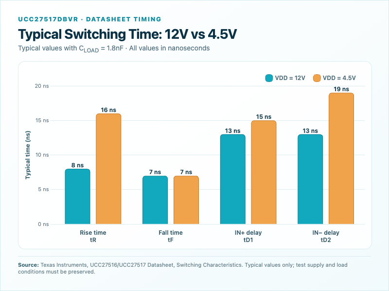
Timing also depends on supply and load. At 12V with a 1.8nF load, the Datasheet table gives 8ns typical rise and 7ns typical fall. At 4.5V, typical rise time doubles to 16ns while the listed typical fall time remains 7ns. Propagation through IN+ is 13ns typical at 12V and 15ns typical at 4.5V; the IN- path is 13ns and 19ns respectively. These results are useful comparison points, not guarantees for a different MOSFET, gate resistor, probe setup or PCB.
| Parameter | Datasheet value | Conditions or design boundary |
|---|---|---|
| Recommended VDD | 4.5V to 18V | Normal operating range |
| Absolute maximum VDD | 20V | Stress rating only; retain transient margin |
| Operating junction temperature | -40°C to +140°C | Absolute maximum junction temperature is +150°C |
| UVLO start threshold | 4.20V typical; 3.70V to 4.65V over temperature | OUT remains low below the applicable threshold |
| UVLO hysteresis | 0.3V typical; 0.2V to 0.5V range | Control supply ripple near the low-voltage boundary |
| Input threshold ranges | High trip 2.2V to 2.4V; low trip 1.0V to 1.2V | For firm logic states, drive above the high range or below the low range |
| Input hysteresis | 1.0V typical | Improves noise immunity but does not correct a poor ground reference |
| Peak source/sink current | +4A / -4A | Pulsed capacitive-load capability; 4A is not continuous |
| Continuous OUT current | 0.3A absolute maximum | Stress boundary, not a recommended DC operating point |
| 12V rise/fall | 8ns / 7ns typical; 12ns / 11ns maximum | CLOAD = 1.8nF |
| 12V propagation | 13ns typical, 23ns maximum for IN+ and IN- paths | 5V input pulse, CLOAD = 1.8nF |
| 4.5V rise/fall | 16ns / 7ns typical; 22ns / 11ns maximum | CLOAD = 1.8nF |
| 4.5V propagation | IN+ 15ns typical/26ns maximum; IN- 19ns typical/30ns maximum | 5V input pulse, CLOAD = 1.8nF |
| UCC27517 DBV RθJA | 217.6°C/W | Standardized package comparison; board design and airflow change real results |
Table 2: UCC27517DBVR electrical and switching specifications with test conditions | Source: TI UCC27516/UCC27517 Datasheet pages 5-7 | Compiled by: icallin.com
IN+, IN-, Enable and UVLO Behavior
The UCC27517DBVR pinout is compact: pin 1 is VDD, pin 2 is GND, pin 3 is IN+, pin 4 is IN- and pin 5 is OUT. The two input pins are not redundant copies. Their logic is combined so OUT goes high only when IN+ is high and IN- is low.
For noninverting operation, apply PWM to IN+ and hold IN- low, normally with a short connection to GND. OUT then follows IN+. If the design needs a separate disable command, IN- can become an active-low enable: low enables switching, while high forces OUT low.
For inverting operation, apply PWM to IN- and hold IN+ high. OUT then produces the inverse of IN-. IN+ can become an active-high enable: high enables switching, while low forces OUT low. This flexibility can remove a separate enable pin, but it also means the unused input must have a defined state.
Internal bias resistors give the device a safe-low behavior when either input floats. That is useful during controller reset or connector faults, but it is not permission to route the unused input casually. TI recommends tying it to the required rail with a short trace in noisy environments. A floating or noise-coupled input disables the output or can create unexpected behavior around ground bounce.
| Item or mode | Pin/state | OUT behavior | Layout or control note |
|---|---|---|---|
| VDD | Pin 1, 4.5V to 18V recommended | Supplies logic and source-current pulses | Decouple directly to pin 2 with 100nF plus a nearby larger capacitor |
| GND | Pin 2 | Reference for input and output voltages | Return to the MOSFET source and controller reference through a short, controlled star path |
| IN+ | Pin 3, noninverting input | High contributes to OUT high; low forces OUT low | Internal pulldown gives safe-low behavior if floating |
| IN- | Pin 4, inverting input | Low contributes to OUT high; high forces OUT low | Internal pullup gives safe-low behavior if floating |
| OUT | Pin 5 | Sources and sinks MOSFET/IGBT gate charge | Keep the OUT-to-gate path short; include the return path in loop optimization |
| Noninverting drive | PWM to IN+; IN- held low | OUT follows PWM after propagation delay | IN- may be used as active-low enable |
| Inverting drive | PWM to IN-; IN+ held high | OUT is inverted after propagation delay | IN+ may be used as active-high enable |
| Both inputs high or both low | Defined logic states | OUT low | Only IN+ high plus IN- low produces OUT high |
| Either input floating | Floating condition | OUT low | Safety behavior; do not rely on a long noisy trace as the bias method |
| VDD below UVLO threshold | Any input state | OUT held low | Startup and shutdown timing must include UVLO thresholds and hysteresis |
Table 3: UCC27517DBVR pin, input-logic, enable and UVLO state guide | Source: TI UCC27516/UCC27517 Datasheet pages 4 and 13-16 | Compiled by: icallin.com
The inputs accept common 3.3V and 5V logic, but edge quality still matters. TI treats a 1nF input capacitor as a worst-case ground-bounce remedy, not a substitute for layout. Use gate-path resistance, not a deliberately slow PWM edge, to control MOSFET slew.
How Much Gate Current Does the MOSFET Need?
The first selection step is not comparing 4A with a MOSFET's continuous drain current. Gate-current demand comes from charge and time. During the Miller plateau, the driver must deliver the gate-drain charge QGD while the drain voltage changes. A useful first-order estimate is:
Required peak gate current ≈ QGD / target Miller time
TI's application example uses a power MOSFET with 33nC typical Miller charge and a target transition time of 20ns. Dividing 33nC by 20ns gives 1.65A. On paper, the 4A source capability is approximately 2.4 times that requirement, leaving room for device variation and an external resistor used to balance efficiency against EMI.
With 33nC QGD, 10ns requires 3.30A, 20ns requires 1.65A, 30ns requires 1.10A and 40ns requires 0.825A. These ideal values exclude output impedance, gate resistance, loop inductance and charge variation.

QGD estimates current during the drain transition; total QG estimates average drive energy. The example uses 87nC total charge, but a new MOSFET requires its own charge curve at the actual VDS, ID and gate voltage. Parasitic inductance can also prevent current from reaching 4A in time, so the calculation never replaces layout validation.
Decoupling and Fast Gate-Loop Layout
Page 23 of the supplied Datasheet shows a UCC27517DBV noninverting layout example. Its most important lesson is geometric: the driver, local bypass network and power MOSFET must be treated as one switching cell.
Place the Driver by the Gate and Source, Not by the Controller
Place UCC27517 close to the MOSFET gate and source reference; a short gate trace with a long return still forms a large loop. Avoid shared load-current impedance where practical so source-copper voltage does not corrupt VGS. This principle does not imply that every MOSFET has a Kelvin-source pin.
Put the 100nF Capacitor Directly Across VDD and GND
Place a 0.1uF low-ESR ceramic directly at pins 1 and 2, then add a nearby low-ESR SMD capacitor of about 1uF or a few microfarads. A remote electrolytic cannot supply the first nanoseconds through its connection inductance. Keep the local capacitor-driver-gate-source loop compact.
Minimize Both Turn-On and Turn-Off Loops
Both charge and discharge loops carry high di/dt, so optimizing only turn-on leaves a weak sink path. Route forward and return conductors together for flux cancellation; trace width cannot rescue paths separated by a large loop area.
Separate Signal Routing From the Power Switching Node
Keep IN+ and IN- away from the drain node and gate-current path. Join driver GND, source reference and controller ground through short, wide controlled paths. A ground plane can shield and spread heat, but it should not become an undefined high-di/dt return loop.
Gate Resistor, Ringing and EMI Trade-Offs
There is no Datasheet-approved universal gate-resistor value. The right resistance depends on the MOSFET's charge, internal gate resistance, target dVDS/dt, driver supply, layout inductance, switch-node capacitance, power-loop behavior and EMI limit.
Start from QGD and the transition target, then include total resistance. The 12V DC table lists 5.0 ohms typical pullup and 0.5 ohm typical pulldown, but the hybrid pullup adds a brief N-channel current boost. The 5-ohm DC ROH value therefore does not describe the complete turn-on transient.
More resistance can reduce ringing and EMI but increase switching loss; too little can cause overshoot and false turn-on. Validate VGS, VDS, OUT and local VDD with a ground spring or differential probe at gate/source. A resistor-diode network may split turn-on and turn-off speeds, but its polarity and fault behavior require circuit-level review.
Thermal and Gate-Drive Power Checks
Average gate-drive demand rises with total gate charge, drive voltage and switching frequency. The Datasheet uses the plain relationship:
Gate-charge power from the bias source ≈ QG x VDD x fSW
For the Datasheet's 87nC example, 12V and 100kHz gives about 0.104W; 500kHz gives about 0.522W. Internal driver resistance, external resistance and the MOSFET share this energy. DBV RθJA is 217.6°C/W, but PCB copper, airflow and nearby heat sources determine actual temperature, so calculate risk and verify the board thermally.
| Design stage | Datasheet-backed check | Pass criterion for the project |
|---|---|---|
| Exact device | Confirm UCC27517DBVR, DBV-5, 3000-piece reel and marking 7517 | Schematic, BOM, footprint, feeder and receiving plan use the same complete OPN |
| Supply | Use 4.5V to 18V recommended range and retain margin below 20V absolute maximum | Local VDD stays inside limits during startup, shutdown and switching transients |
| High-frequency bypass | Place 100nF low-ESR ceramic directly at VDD/GND | Connection is short, low inductance and inside the gate-current cell |
| Local energy storage | Add roughly 1uF or a few microfarads low-ESR SMD in parallel nearby | Local rail droop does not trigger UVLO or distort gate amplitude |
| Driver placement | Put the driver close to MOSFET gate and source reference | OUT/gate and source/GND paths form a tight forward/return pair |
| Grounding | Use short, wide controlled star connection; separate signal and power routing | Load-current or switch-node noise does not modulate the input reference |
| Unused input | Tie IN- low for noninverting mode or IN+ high for inverting mode | No uncontrolled floating or long noise-sensitive trace |
| Gate resistance | Select from QGD, transition target and measured ringing/loss | VGS/VDS slew, overshoot, EMI and switching loss all meet limits |
| Thermal | Estimate QG x VDD x fSW and account for resistance sharing | Measured temperature remains below the project junction-temperature limit at worst case |
| Bench validation | Probe VGS at gate/source with low-inductance technique; observe VDS, OUT and VDD | No destructive overshoot, false switching, UVLO chatter or thermal runaway |
Table 4: UCC27517DBVR schematic, decoupling, PCB layout, thermal and bench-validation checklist | Source: TI UCC27516/UCC27517 Datasheet pages 19-25 | Compiled by: icallin.com
Applications: SMPS, DC-DC, Solar, Motor Control, UPS and GaN
The Datasheet explicitly lists switched-mode power supplies, DC-DC converters, companion gate-driver use with digital power controllers, solar power, motor control, UPS systems and emerging wide-bandgap devices such as GaN.
The driver can translate a 3.3V controller PWM into a higher-current gate pulse for SMPS, DC-DC, solar, UPS or low-side motor stages. It is not an isolated half-bridge driver; a floating or high-side N-channel switch needs the appropriate high-side or isolated architecture.
GaN requires an additional voltage check. TI highlights operation below 5V and specifically identifies emerging GaN devices, but it also warns that some wide-bandgap gates allow no more than about 6V. The selected transistor's allowed gate range, recommended turn-on voltage, negative transient limit and source inductance must govern the final design. The 4.5V minimum UCC27517 supply and the actual OUT overshoot must both fit inside that gate window.
Related methods appear in ICAllin's MOSFET gate-drive discussion, low-side-driver qualification guide, battery-management sourcing guide and remote-sensor power guide.
Five-Model Qualification Matrix
| Role | Exact model | Key documented difference | Qualification boundary | ICAllin route |
|---|---|---|---|---|
| Primary baseline | UCC27517DBVR | Active 4A/4A, 13ns typical, 4.5V to 18V, dual-input SOT-23-5; 3000 large T&R | Original UCC27517 input record; no documented -5V input handling | UCC27517DBVR |
| Packing-only option | UCC27517DBVT | Same UCC27517 DBV electrical device; 250 small T&R | Electrical design is unchanged, but carrier quantity and exact OPN differ | UCC27517DBVT |
| Negative-input upgrade path | UCC27517ADBVT | UCC27517A adds documented -5V input handling; 4A/4A and 13ns typical; 250 small T&R | TI identifies UCC27517A as a newer functional upgrade, but exact Datasheet, packing and program limits must be approved | UCC27517ADBVT |
| Automotive path | UCC27517AQDBVRQ1 | AEC-Q100 Grade 1, -5V input handling, SOT-23-5; 3000 large T&R | Automotive qualification and controlled documentation belong only to the Q1 OPN | UCC27517AQDBVRQ1 |
| Thermal/footprint redesign | UCC27516DRSR | Same 4A/4A and 13ns family architecture; 6-pin 3mm x 3mm WSON, exposed pad; RθJA 85.6°C/W | Not footprint-compatible; new pin map, land pattern, exposed-pad grounding and assembly qualification required | UCC27516DRSR |
Table 5: UCC27517DBVR and four TI gate-driver qualification paths | Source: Current TI product/order pages and Datasheets | Compiled by: icallin.com
Current Status and Sourcing Checks
As checked on August 2, 2026, TI marks the exact OPN Active and lists 3000 pieces per reel, MSL Level 1, RoHS Yes and marking 7517. A purchase record should still specify quantity, carrier, date/lot policy, traceability, labels and storage. If DBVT, UCC27517A, Q1 or WSON is offered, record whether the change is packing, silicon behavior, qualification or footprint.
FAQs
1. Is UCC27517DBVR still Active, and what does the R suffix mean?
TI's current product and exact-order pages identify UCC27517DBVR as Active, and the July 22, 2026 package addendum lists it as Active Production. The R carrier is the 3000-piece large tape-and-reel version. Active status does not establish today's distributor inventory, price, date code or delivery time.
2. What are the main UCC27517DBVR features and Datasheet applications?
The key features are 4A peak source and 4A peak sink at VDD = 12V, 13ns typical propagation delay, 4.5V to 18V operation, fixed TTL/CMOS-compatible input thresholds, inverting/noninverting control, UVLO and safe-low floating-input behavior in SOT-23-5. TI lists SMPS, DC-DC converters, digital power controllers, solar power, motor control, UPS and suitable GaN drive as applications.
3. How close should UCC27517DBVR be placed to the MOSFET, and how should the gate loop be routed?
Place it as close as practical to both the MOSFET gate and the source reference. Minimize the complete loop formed by the local bypass capacitor, VDD, driver OUT, MOSFET gate/source and driver GND. Route forward and return paths together, separate the input from switching nodes and connect the driver ground through a short, wide controlled star path.
4. What bypass capacitors and gate resistor should be used with UCC27517DBVR?
TI recommends a 100nF low-ESR ceramic directly across VDD and GND plus a nearby low-ESR surface-mount capacitor of about 1uF or a few microfarads. There is no universal gate-resistor value. Select it from QGD, target switching time, loop impedance and measured VGS/VDS ringing, switching loss and EMI.
5. How do IN+, IN-, enable/disable and UVLO work on UCC27517DBVR?
For noninverting drive, apply PWM to IN+ and hold IN- low; IN- can act as active-low enable. For inverting drive, apply PWM to IN- and hold IN+ high; IN+ can act as active-high enable. OUT is high only when IN+ is high and IN- is low. A floating input or an active UVLO condition forces OUT low.
6. Can UCC27517DBVT, UCC27517ADBVT, UCC27517AQDBVRQ1 or UCC27516DRSR directly replace UCC27517DBVR?
DBVT is the same UCC27517 DBV electrical device with a 250-piece small-reel carrier, so its documented difference is packing. UCC27517A adds negative-input capability, Q1 adds automotive qualification and UCC27516DRSR changes to a 6-pin exposed-pad WSON. Each exact OPN still requires BOM, package, input, temperature, qualification and production review before approval.
Immediate Stock Alert
Active is a manufacturer lifecycle label, not proof of current ICAllin stock. Availability, price, lead time, date code and lot structure can change between checks. Use the UCC27517DBVR product page to identify the exact model, then submit the required quantity, carrier, delivery destination, date-code policy and traceability requirements through the ICAllin request page for a dated commercial response.
Do not accept a substitution based only on the UCC27517 family name. A response should state whether the offered material is DBVR, DBVT, an A device, Q1 or UCC27516 WSON and should separate engineering approval from commercial availability.
Conclusion
UCC27517DBVR combines a useful 4A/4A peak output stage, 13ns typical propagation, dual-input control and a 4.5V to 18V supply range in SOT-23-5. Those specifications make it a strong low-side drive option for SMPS, DC-DC, solar, UPS, motor-control and carefully selected GaN designs.
The decisive design variable is the current loop. A 100nF capacitor at the pins, nearby microfarad-level support, a short driver-to-gate path, a short source return and controlled grounding allow the output stage to move charge quickly. A long or shared loop can erase the current margin predicted by QGD divided by switching time.
Treat the Datasheet numbers as conditioned engineering inputs, not slogans: 4A is peak, 18V is the recommended ceiling, 20V is an absolute maximum, and timing depends on VDD and load. Finally, keep DBVR, DBVT, UCC27517A, Q1 and UCC27516DRSR separated by their exact electrical, qualification, package and packing records. That discipline connects the PCB layout, bench validation and purchasing decision into one controlled design.
References
- Texas Instruments, UCC2751x Single-Channel, High-Speed, Low-Side Gate Driver (With 4-A Peak Source and 4-A Peak Sink), Rev. D, supplied Datasheet and current package addendum: https://www.ti.com/lit/ds/symlink/ucc27517.pdf
- Texas Instruments, UCC27517 product page: https://www.ti.com/product/UCC27517
- Texas Instruments, UCC27517DBVR exact order page: https://www.ti.com/product/UCC27517/part-details/UCC27517DBVR
- Texas Instruments, UCC27517A product page: https://www.ti.com/product/UCC27517A
- Texas Instruments, UCC27517A-Q1 product page: https://www.ti.com/product/UCC27517A-Q1
- Texas Instruments, UCC27516 product page: https://www.ti.com/product/UCC27516
- ICAllin, UCC27517DBVR product page: https://icallin.com/product-detail/texas-instruments-ucc27517dbvr
- ICAllin, Texas Instruments manufacturer page: https://icallin.com/manufacturers/texas-instruments
- ICAllin, Current availability request page: https://icallin.com/rfq


Top Recommended part