XC7Z045-2FFG900I: Stream CT Data Before AI Analysis
Category: Industry Applications & Solutions | Author: Klaus·Fische | Primary MPN: XC7Z045-2FFG900I | Manufacturer: AMD Xilinx | Source checked: August 8, 2026
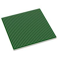
XC7Z045-2FFG900I is an industrial Zynq-7000 SoC that combines dual Arm Cortex-A9 processing with a large programmable-logic fabric in a 900-ball FFG package. Its fabric provides 900 DSP slices and 19.2 Mb of block RAM, while four AXI high-performance ports can move detector streams toward shared memory. This guide shows how to preprocess CT data deterministically before handing selected images or features to downstream AI.
Catalog
- Key Takeaways
- Evidence and Exact-OPN Scope
- Decode XC7Z045-2FFG900I
- Why Stream CT Data Before AI
- Map Z-7045 Resources to the Pipeline
- Design the PS–PL Data Path
- Build a CT Streaming Budget
- Preserve Image and Debug Evidence
- Compare the First Five W32 Devices
- Implementation and Bring-Up Gates
- Lifecycle and Procurement
- Frequently Asked Questions
- Immediate Stock Alert
- Conclusion
- References
Key Takeaways
- XC7Z045-2FFG900I gives a CT design two complementary execution domains: programmable logic for deterministic, sample-by-sample work and dual Cortex-A9 processing for configuration, supervision, exception handling and software-visible control.
- The exact Z-7045 fabric contains 218,600 LUTs, 437,200 flip-flops, 900 DSP slices and 545 36 Kb block-RAM blocks. Those are available resources, not proof of an achieved CT rate or neural-network performance.
- FFG900 exposes 128 PS I/Os, 212 HR PL I/Os, 150 HP PL I/Os and 16 GTX lanes. The package facts do not include the memories, connectors, clocks or power circuitry shown in the ZC706 board guide.
- Four AXI high-performance ports can carry PL traffic toward processing-system memory, but delivered bandwidth depends on width, clock, bursts, arbitration, DDR efficiency and backpressure. Port count alone is not a throughput guarantee.
- XCN20011 maps discontinued XC7Z045-2FFV900I to XC7Z045-2FFG900I. That notice must not be reversed into a claim that the FFG900I replacement is discontinued.
- “Before AI” means deterministic conditioning and controlled data reduction before a separately qualified AI stage. XC7Z045 has no AI Engine, and this article does not invent one.
Evidence and Exact-OPN Scope
This is a doc-review; no hardware, CT detector, bench throughput, image-quality or AI-accuracy result was supplied. The AMD/Xilinx sources are used only within their stated roles. 第三篇.pdf and 第三篇-1.pdf are duplicate copies of XCN20011. Page 4, Table 6 names XC7Z045-2FFG900I as the replacement for XC7Z045-2FFV900I. The notice is a transition record for the older FFV OPN, not the FFG900I electrical data sheet or a present inventory report.
Three other supplied files are customer engineering-sample errata. Their CES identifiers and workarounds belong to the specific engineering-sample scope stated in those documents. A production article should not quietly turn a CES condition into a feature, limitation or required workaround for XC7Z045-2FFG900I. Those files are used here to demonstrate evidence control, not to fill gaps in the production OPN.
The largest supplied file is UG954, the ZC706 evaluation-board guide. That board is highly relevant as a system example, but it contains XC7Z045-2FFG900C, not the industrial XC7Z045-2FFG900I. Its DDR memory, flash, clocks, connectors, power rails, transceivers and layout are properties of a specific board. They do not become resources inside the target SoC, and its schematic cannot be copied as the exact FFG900I design without a new package, temperature, memory and board review.
The technical baseline comes from DS190 for Z-7045 resources and package exposure, DS191 for exact DC/AC switching limits, UG865 for FFG900 mechanics and ball assignments, and UG585 for processing-system and PS–PL architecture. AMD's CT/MRI solution page and Mindray case study establish medical-imaging application context, not a diagnostic result, certified system, detector rate or exact-OPN performance.
The title is therefore an architecture argument, not a performance claim. It cannot promise slices per second, image quality, reconstruction latency, regulatory acceptance or AI accuracy without an implemented system and measured evidence.
Decode XC7Z045-2FFG900I
The orderable part number belongs in the architecture record, Vivado project, schematic, BOM, approved-vendor list, programming instructions and incoming-inspection plan. Writing only XC7Z045 discards the speed grade, package and temperature suffix that control implementation and procurement.
XC7Z identifies a Zynq-7000 device that combines a processing system and 7 Series programmable logic. 045 selects the Z-7045 capacity. -2 selects the speed-grade column that must control timing and interface limits in the applicable AMD data sheet. FFG900 identifies the 900-ball flip-chip package variant used here, with a 31 × 31 mm body and 1.0 mm ball pitch. The final I is the industrial junction-temperature grade, Tj = -40°C to +100°C. It is not a promise that every board component or enclosure may operate at the same ambient extremes.
The supplied XCN adds a second identity lesson. FFV900I and FFG900I are not interchangeable strings. XCN20011 explicitly records a change path from the discontinued FFV OPN to the FFG OPN. Engineering still has to compare package documentation, assembly controls, qualification records and any applicable notice conditions. Procurement must order the full target OPN, not silently substitute whichever three-letter package code appears in a channel listing.
| Code or evidence field | Controlled meaning | Exact boundary used in this article | Engineering consequence |
|---|---|---|---|
| XC7Z | AMD/Xilinx Zynq-7000 SoC family | Dual-domain PS plus 7 Series PL architecture | Selects architecture, tools and document family |
| 045 | Z-7045 device | 350,000 logic cells, 900 DSP slices and 545 BRAM blocks | Sets silicon capacity, not package-exposed connectivity |
| -2 | Speed grade | Exact timing column must be used in implementation | Re-run timing whenever the speed code changes |
| FFG900 | 900-ball FFG package | 31 × 31 mm, 1.0 mm pitch and exact package I/O exposure | Controls footprint, escape, pinout, thermal and assembly work |
| I | Industrial temperature grade | Tj = -40°C to +100°C | Validate junction temperature and all board components separately |
| XCN20011 | Product-change/discontinuance notice | Maps XC7Z045-2FFV900I to XC7Z045-2FFG900I | Do not call the replacement OPN discontinued because it appears in the notice |
| UG954 | ZC706 board guide | Board uses XC7Z045-2FFG900C | Board resources and the commercial suffix remain outside target OPN facts |
| CES errata | Engineering-sample history | Applies only to the identified CES material | Do not transfer workarounds to production without exact evidence |
Table 1: XC7Z045-2FFG900I order-code and evidence-scope decoder | Source: AMD/Xilinx DS190, UG865, XCN20011 and UG954 | Compiled by: icallin.com
This discipline prevents two expensive errors: designing to resources that live on an evaluation board rather than in the chip, and approving a related suffix without reopening the technical and commercial qualification.
Why Stream CT Data Before AI
A CT acquisition path starts as a continuous, ordered flow of detector samples. Many early operations are deterministic: lane alignment, bad-channel masking, offset and gain correction, dark-field subtraction, range checks, fixed filtering, binning, formatting, timestamping and integrity tagging. Those operations are naturally expressed as pipelines because each sample can move forward as soon as its required neighborhood or calibration state is available.
Waiting for a complete frame or view before every operation creates avoidable buffering and software scheduling. A programmable-logic pipeline can accept the next sample while earlier samples occupy later stages. Block RAM can hold line windows, coefficients, delay alignment and small working sets. DSP slices can implement multiply-accumulate and fixed-point arithmetic. LUTs and flip-flops can provide protocol state, data selection, counters and custom control. The dual Cortex-A9 system can configure coefficients, supervise status, handle exceptions and manage the broader software state.
This is not an argument for discarding raw data. A medical-imaging design needs traceability and an auditable path between acquired data, corrections and output. The architecture should therefore define which stream is lossless, which transformations are reversible, which reductions are permitted, and when a bypass or raw-capture path is activated. Calibration identifiers, coefficient versions, saturation flags, dropped-sample counters and timestamps should travel with the data or be stored in a synchronized record.
The downstream AI boundary also needs precision. XC7Z045-2FFG900I does not contain the AI Engine array found in later AMD device families. “Before AI” can mean that the SoC prepares normalized images, regions, projections or quality flags for an external accelerator, server or separately implemented inference design. It can also mean that conventional reconstruction and visualization receive the conditioned stream while AI consumes a controlled copy. The exact partition depends on latency, data-retention, privacy, serviceability and regulatory requirements.
The strongest reason to preprocess first is therefore not a fashionable AI label. It is system determinism. The acquisition path should remain bounded and observable even when Linux, networking, storage or a downstream model experiences variable latency. Backpressure must have a defined response: buffer within a proven limit, throttle acquisition through an approved mechanism, switch to a safe mode, or raise a recorded fault. Silent data loss is not an architecture.
Map Z-7045 Resources to the Pipeline
The Z-7045 programmable logic offers 218,600 LUTs, 437,200 flip-flops, 900 DSP slices and 545 36 Kb block-RAM blocks, approximately 19.2 Mb in aggregate. DS190 also describes 350,000 vendor-equivalent logic cells. Logic cells are an AMD capacity metric; they are not an additional pool that can be added to the LUT and flip-flop counts.
The processing system contains two Cortex-A9 cores, 32 KB instruction and 32 KB data L1 cache per core, 512 KB shared L2 cache and 256 KB on-chip memory. These resources can run software control and data-management functions, but the maximum 800 MHz processor figure is not an application benchmark. Cache behavior, memory traffic, interrupts, operating system and software design determine delivered performance.
Map resources by timing behavior. Use PL state and counters for cycle-bounded protocol handling. Use DSP slices where coefficients, precision and throughput justify hard arithmetic. Use BRAM for short deterministic buffers and line windows. Use the PS for configuration, policy, metadata, health monitoring and tasks whose latency can vary within a defined bound. If software must touch every detector sample to keep the pipeline moving, the design has likely moved a deterministic responsibility into a variable-latency domain.
| Resource | Exact Z-7045 value | Suitable CT-pipeline roles | Claim boundary |
|---|---|---|---|
| Cortex-A9 cores | 2, up to 800 MHz | Configuration, supervision, metadata, network/storage orchestration | Not a measured application rate |
| L1 cache | 32 KB instruction + 32 KB data per core | Low-latency code and working data | Cache hit rate depends on software and traffic |
| Shared L2 / OCM | 512 KB / 256 KB | Shared control data, descriptors and bounded low-latency storage | Not a replacement for a full acquisition buffer |
| Logic cells | 350,000 | Vendor capacity comparison | Do not add to physical LUT/FF counts |
| LUTs / flip-flops | 218,600 / 437,200 | Stream control, custom datapaths, alignment and status | Available, not utilized, resources |
| DSP slices | 900 | Correction, filtering and fixed-point multiply-accumulate | No implied TOPS or CT throughput |
| 36 Kb BRAM blocks | 545, about 19.2 Mb total | Line windows, coefficient stores, FIFOs and short buffers | External memory still required for deeper storage |
| DMA channels | 8, including 4 dedicated to PL | Descriptor-driven data movement | Delivered rate requires measurement |
Table 2: Z-7045 processing-system and programmable-logic resource baseline | Source: AMD/Xilinx DS190 and UG585 | Compiled by: icallin.com

The chart must show counts with explicit resource labels. It must not combine them into a score, imply they are consumed by this article's conceptual pipeline, or convert the DSP count into an unsupported AI-performance figure.
Design the PS–PL Data Path
Zynq-7000 exposes several PS–PL interfaces because control, bulk data and coherent acceleration have different needs. The two 32-bit general-purpose master ports let the PS address PL registers and lightweight peripherals. The two 32-bit general-purpose slave ports allow PL masters to access PS address space. These paths are well suited to configuration, status and moderate control transactions; they should not be chosen for a detector stream merely because they are easy to address.
Four high-performance slave ports accept PL masters and provide a path toward PS memory resources. Each supports 64- or 32-bit operation under the architecture. A DMA engine in PL or an appropriate PS/PL design can issue bursts, maintain multiple buffers and signal completion through interrupts. The 64-bit accelerator coherency port is valuable when PL-generated data must participate in the processor cache-coherency domain, but coherency is not free. The software mapping, cache policy, barriers, descriptor ownership and buffer lifecycle must be designed as one system.
The theoretical width of four HP ports should never appear as a guaranteed aggregate bandwidth. At minimum, calculate the active width and clock of each path, protocol overhead, burst length, outstanding transactions, arbitration, DDR-controller scheduling, refresh, bank conflicts and competing CPU/PL traffic. Then measure sustained and worst-window behavior using counters at the input, DMA, AXI path, memory controller and consumer. A high average can still conceal a short stall that overflows an acquisition FIFO.
Interrupts should report events rather than carry the data path. Use them for buffer completion, threshold crossing, calibration changes and faults. Rate-limit or coalesce routine completions when appropriate, and provide counters that reveal missed or delayed service. If the application requires an interrupt for every small packet, test the worst-case service latency under the approved operating-system load.
Package exposure matters too. FFG900 provides 128 PS I/Os, 212 HR PL I/Os, 150 HP PL I/Os and 16 GTX lanes. Those counts describe available package connectivity before the design consumes configuration, clocks, memory, references and interfaces. They do not describe ZC706 connectors or prove that a proposed detector interface fits particular banks.
| Interface or package resource | Exact count/width | Recommended role in this architecture | Verification needed |
|---|---|---|---|
| AXI GP master | 2 × 32-bit | PS configuration and PL register access | Address map, ordering and timeout behavior |
| AXI GP slave | 2 × 32-bit | PL access to selected PS address space | Security, ownership and traffic bound |
| AXI HP slave | 4 × 64/32-bit | Burst movement from PL toward shared memory | Clock, width, bursts, arbitration, DDR efficiency and backpressure measurement |
| Accelerator coherency port | 1 × 64-bit | Coherent accelerator buffers when software truly needs them | Cache policy, barriers, ownership and coherency validation |
| PL-to-PS interrupts | 16 | Completion, health and fault events | Worst-case service latency and event-loss test |
| PS I/O | 128 | Processing-system peripheral connectivity | Exact pinout and bank review |
| HR / HP PL I/O | 212 / 150 | Detector, memory and custom interface planning | Voltage, bank, clock and package-pin constraints |
| GTX lanes | 16 | Up to 10.3125 Gb/s for -2I FF | Protocol, reference clock, channel and SI validation |
Table 3: FFG900 package exposure and XC7Z045 PS–PL data-path baseline | Source: AMD/Xilinx DS190, DS191, UG865 and UG585 | Compiled by: icallin.com
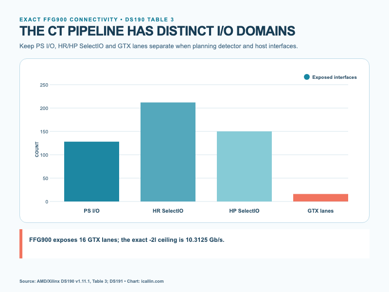
The connectivity chart is a package-planning view. Because I/O pins and transceiver lanes serve different electrical functions, the visual must not turn their sum into one interchangeable total.
Build a CT Streaming Budget
Begin with the detector contract, not the FPGA headline. Record active channels, samples per channel, bits per sample, acquisition events or views per second, packet or framing overhead, calibration traffic and any duplicated safety stream. The raw payload rate is active channels multiplied by samples per event, bytes per stored sample and events per second. Add framing and transport overhead separately so that changes remain visible.
Next define every transformation. A correction may preserve sample count but widen the internal word. A filter may require a neighborhood and line storage. Binning or region selection may reduce the outbound rate. Metadata and integrity tags add data. A diagnostic raw-capture mode may temporarily remove the reduction that made the nominal path comfortable. Calculate nominal, worst-approved and fault/diagnostic cases rather than one average.
For each FIFO, write its producer rate, consumer rate, maximum allowed stall, depth, almost-full response and overflow behavior. A simple sizing check is buffer bytes = peak excess bytes per second multiplied by maximum stall seconds, plus implementation margin. The approved stall must come from measured downstream behavior or a controlled requirement. Choosing a larger FIFO without defining what happens when it fills merely delays the same failure.
The memory budget must include DDR efficiency. Requested bytes divided by theoretical bus capacity is not the same as delivered utilization. Include bursts, row behavior, refresh, arbitration, CPU traffic, descriptors and readback. If AI, reconstruction, display and storage read the same data, decide whether copies are required, whether buffers can be shared coherently, and who owns each transition. Use double or ring buffering only with explicit producer/consumer ownership states.
Finally, preserve latency by stage. Measure detector input to corrected output, corrected output to memory completion, memory completion to consumer availability and any downstream response. An end-to-end average cannot reveal which stage occasionally violates the limit. Hardware counters, timestamps and watermarks should make the stream observable without an external logic analyzer.
Preserve Image and Debug Evidence
Deterministic does not mean infallible. Fixed-point arithmetic needs a documented range at every stage, coefficient scaling, rounding rule, saturation behavior and overflow flag. Compare the bit-accurate hardware model with a trusted reference using representative, boundary and corrupted inputs. Store the coefficient set and algorithm revision with each qualification result.
Provide controlled bypasses. A stage-level bypass can isolate whether an artifact is introduced by calibration, filtering, data movement or software. A raw-capture mode can retain selected detector data for comparison, but its bandwidth and privacy implications must be included in the architecture. A synthetic-pattern generator can test transport independently of the detector. CRCs, sequence numbers and timestamps can distinguish calculation errors from lost, duplicated or reordered transfers.
Expose health through counters for input/output words, overflow, dropped packets and resets. Latch the first fault context and define how it clears without losing evidence.
Medical-system teams also need configuration control. Tie the FPGA bitstream, software build, calibration set, board revision, detector revision and test dataset together. A result obtained with an engineering-sample device, ZC706 board or commercial-temperature OPN cannot silently qualify the final industrial production assembly.
Compare the First Five W32 Devices
The first five W32 articles form a closed comparison set. That makes them useful architectural reference points, but it does not turn them into replacements. XC7Z020 and XC7Z030 can show how a smaller Zynq-7000 design changes the PL budget. XCZU3EG adds A53, R5F and GPU domains for heterogeneous edge control. XCZU7EV adds an EV-class video-oriented path. Every change reopens package, power, clocks, interfaces, software, bitstream, performance and validation.
| Role | Exact model | Architectural comparison question | Non-substitution boundary |
|---|---|---|---|
| Primary CT-stream baseline | XC7Z045-2FFG900I | How should dual A9 plus large 7 Series PL condition detector data before AI? | Only this row carries the exact resources and package facts in this article |
| Smaller Zynq-7000 | XC7Z020-1CLG400C | Can a lower-resource PS/PL design meet the measured stream budget? | Different speed, package, temperature and resources require a new implementation |
| Mid-range Zynq-7000 | XC7Z030-2FBG676I | Does the workload fit a smaller streaming/DSP partition? | FBG676 and device resources are not pin- or capacity-equivalent |
| EG MPSoC | XCZU3EG-1SFVC784I | Would separate A53, R5F and PL domains improve control and fusion? | New generation, package, tools and software stack mean system redesign |
| EV MPSoC | XCZU7EV-2FFVC1156I | Does the application require an integrated video-oriented pipeline? | Different device/subfamily, package and qualification; no automatic migration |
Table 4: First-five W32 architecture comparison matrix for XC7Z045-2FFG900I | Source: AMD/Xilinx DS190, DS891 and verified ICAllin product routes | Compiled by: icallin.com
Select another row only after requirements change. The decision needs an I/O map, data-rate budget, execution-domain plan, memory design, software impact and validation cost.
Implementation and Bring-Up Gates
Start with a bit-accurate software or model-based reference for each preprocessing stage. Verify individual RTL blocks with normal, boundary, stalled and corrupt input. Then verify the integrated AXI stream under randomized backpressure. Assertions should catch protocol violations, dropped handshakes and illegal state transitions. Counters at every boundary should reconcile the number of accepted and emitted samples.
Implementation sign-off includes clock-domain crossings, resets, timing, utilization and physical congestion. Treat a timing waiver or asynchronous reset exception as an engineering decision with an owner and proof. Review BRAM/DSP placement and AXI routing; a design can fit numerically yet fail timing or create localized congestion.
Board bring-up should separate the data source, pipeline and memory system. Use an internal pattern first, then a known external pattern, then the detector. Stress DDR and AXI with simultaneous CPU and PL traffic. Force downstream stalls to the approved maximum. Verify that almost-full responses occur early enough and that a true overflow produces a detectable, safe system response.
Temperature and power testing must use measured junction estimates and the complete board. The I suffix applies to the SoC junction range, not to every regulator, memory or connector. Test cold and hot start, warm reset, power interruption, clock loss and software restart. Retain results by exact FPGA OPN, board revision and component lot.
| Gate | Evidence retained | Required challenge | Release criterion |
|---|---|---|---|
| Algorithm reference | Bit-accurate model, coefficient/version record and golden vectors | Boundary, saturation, corrupt and representative CT data | Hardware output matches the approved reference and error policy |
| RTL/stream verification | Assertions, coverage and input/output counts | Random backpressure, resets and malformed packets | No protocol violation, silent loss or unowned state |
| PS–PL integration | Address map, DMA descriptors, ownership and cache policy | Concurrent CPU, PL and memory traffic | Sustained and worst-window rates meet the written budget |
| Implementation | Timing, CDC, reset, utilization and placement reports | All approved clocks and operating modes | No unexplained critical warning or unproven exception |
| Board data path | Pattern generator, detector capture, DDR stress and counters | Maximum approved stall and diagnostic raw-capture mode | No overflow; fault response is observable and safe |
| Image integrity | Golden comparison, metadata, timestamps and error flags | Calibration changes, bypasses and injected errors | Output and provenance remain traceable |
| Environmental behavior | Voltage, junction-temperature and reset logs | Cold/hot start, warm reset and supply/clock disturbance | Repeatable recovery across approved conditions |
| Pilot and incoming control | Exact OPN, lot/date code, board revision and test result | Multiple boards and component lots | Consistent results and closed deviations before release |
Table 5: XC7Z045-2FFG900I CT pipeline implementation and validation evidence record | Technical basis: AMD/Xilinx DS190 and UG585; validation actions are ICAllin-authored engineering recommendations | Compiled by: icallin.com
Release the design only when the evidence chain is reproducible. A demonstration on ZC706 is valuable learning, but it is not the industrial production-board qualification.
Lifecycle and Procurement
XCN20011 provides a precise historical statement: the FFV900I OPN was included in the discontinuance scope and FFG900I was the named replacement. It does not provide today's stock, price, date code or lead time. It also does not eliminate engineering review of the package transition. Keep the notice with the change record and verify any later AMD notices that apply to the full target OPN.
Use the complete XC7Z045-2FFG900I string in every inquiry. Ask for manufacturer, quantity, package, lot/date code, packaging format, moisture handling, traceability and applicable PCN/PDN history. Compare the purchase order, outer label, inner label and device marking at incoming inspection. Link the accepted lot to programming and board-test results.
The AMD Xilinx manufacturer route helps navigate related devices, but a related route is not substitution approval. If engineering is willing to discuss another first-five W32 device, state that separately as a redesign option rather than allowing an informal suffix swap.
Frequently Asked Questions
1. What does XC7Z045-2FFG900I mean?
XC7Z identifies the Zynq-7000 SoC family, and 045 selects the Z-7045 device. -2 is the speed grade used for timing limits. FFG900 identifies the 900-ball package; DS190 supplies its exposure, UG865 its mechanics and pinout, and DS191 the applicable switching limits. The final I is the industrial junction-temperature grade, Tj = -40°C to +100°C. It does not qualify the whole board.
2. Does XC7Z045-2FFG900I contain an AI Engine?
No. XC7Z045 combines dual Cortex-A9 processing with 7 Series programmable logic, DSP slices and block RAM. It does not contain the AI Engine array associated with later AMD architectures. The phrase “before AI analysis” describes an architectural handoff: the SoC can condition, filter, buffer, tag or reduce detector data before a separately qualified accelerator, server or inference implementation consumes it. Any AI function built in PL still needs its own resource, precision, performance and accuracy evidence.
3. Why preprocess CT detector data in programmable logic?
Early detector operations are often ordered, repetitive and timing-sensitive. Programmable logic can pipeline calibration, masking, fixed filtering, windowing, integrity checks and formatting as samples arrive, rather than waiting for a complete frame and a software scheduling event. That can bound latency and reduce unnecessary memory traffic. The design must still preserve raw capture or bypass where required, document fixed-point behavior, carry timestamps and error flags, and prove that no clinically relevant information is silently discarded.
4. How should the four AXI HP ports be used and measured?
Use HP ports for burst-oriented PL masters moving data toward processing-system memory, with DMA descriptors and explicit buffer ownership. Do not multiply four ports by 64 bits and publish the result as achieved bandwidth. Measure the active width and clock, burst efficiency, outstanding transactions, arbitration, DDR scheduling, refresh, competing traffic and backpressure. Instrument input, DMA, AXI, memory and consumer boundaries so both sustained rate and worst-window stalls are visible.
5. Does XCN20011 say XC7Z045-2FFG900I is discontinued?
No. In the supplied notice, Table 6 maps discontinued XC7Z045-2FFV900I to XC7Z045-2FFG900I as the replacement. The distinction between FFV and FFG is essential. XCN20011 is historical change evidence and should be reviewed with any later exact-OPN notices, but it must not be inverted into an FFG900I discontinuance claim. Current commercial availability still requires a dated check.
6. Can any of the four related W32 devices replace XC7Z045-2FFG900I directly?
No comparison device is presented as a drop-in replacement. XC7Z020 and XC7Z030 have different capacity, speed/package combinations and board implications. XCZU3EG and XCZU7EV move to a different MPSoC generation, processing architecture, package, power design, tools and software stack. Use them to ask whether requirements justify a redesign. Any move requires exact data-sheet comparison, schematic and PCB review, new implementation, software changes and complete validation.
Immediate Stock Alert
For a current commercial check, use the exact XC7Z045-2FFG900I product route and submit a dated availability request. Include required quantity, target delivery window, destination, package/packaging needs, lot/date-code preferences, traceability documents and applicable change-notification requirements. Ask the response to preserve the full FFG900I suffix. Do not accept FFV900I, FFG900C or another first-five W32 model without written engineering approval. Availability, price and schedule remain valid only for the dated response.
Conclusion
XC7Z045-2FFG900I supports a sound CT architecture when its two domains have explicit responsibilities. Programmable logic can keep calibration, filtering, buffering and integrity work deterministic; dual Cortex-A9 processing can configure, supervise and orchestrate the wider system. The exact device provides 900 DSP slices and 545 BRAM blocks, while FFG900 exposes the package connectivity and four HP ports create routes toward shared memory. None of those facts guarantees an application rate.
The design becomes credible when it budgets every stream, defines backpressure, measures PS–PL and DDR behavior, preserves provenance and survives reset and environmental testing. “Before AI” is a determinism boundary, not an invented AI Engine. Keep every supplied document in scope and the full OPN connected from Vivado through incoming inspection.
References
- AMD/Xilinx DS190, Zynq-7000 SoC Overview — Z-7045 processing, PL resources, package exposure and application scope.
- AMD/Xilinx DS191, XC7Z030/XC7Z035/XC7Z045/XC7Z100 DC and AC Switching Characteristics — exact speed-grade and temperature switching limits.
- AMD/Xilinx UG865, Zynq-7000 SoC Packaging and Pinout — FFG900 mechanics, pinout and ball assignments.
- AMD/Xilinx UG585, Zynq-7000 SoC Technical Reference Manual — processing system, DMA and PS–PL interfaces.
- Supplied AMD/Xilinx XCN20011,
/Users/liuchen/Downloads/AI Files/icallin_blog/Datasheet/第三篇.pdf— exact FFV900I-to-FFG900I replacement mapping. - Supplied AMD/Xilinx UG954,
/Users/liuchen/Downloads/AI Files/icallin_blog/Datasheet/第三篇-5.pdf— ZC706 board context using XC7Z045-2FFG900C. - AMD CT scanners and MRI solutions — application-level CT/MRI architecture context.
- AMD Mindray case study — medical-imaging application context, not an exact-OPN benchmark.
- ICAllin XC7Z045-2FFG900I product route — exact procurement identity and current inquiry route.
- ICAllin AMD Xilinx manufacturer route and availability request — portfolio navigation and dated commercial review.
Step 2 Dynamic Alignment Record
- The H1, Meta Title and body retain the approved “Stream CT Data Before AI Analysis” decision.
- The 150-character Meta Description is supported: dual Cortex-A9, 900 DSP slices and AXI HP ports appear in the resource/data-path sections and Tables 2–3.
- The 64-word visible intro is reproduced exactly and its package, BRAM, port and application claims are supported.
- XCN20011 is treated as an FFV900I-to-FFG900I mapping; UG954 board resources and CES errata remain outside exact production-OPN parameters.
- Related models are limited to the first-five W32 closed loop and used only for architecture comparison.
- Structural audit result: no Markdown H1, exactly five source-bearing tables, two exact-data figure placeholders and six FAQs.
- Step 3 assets are complete.


Top Recommended part