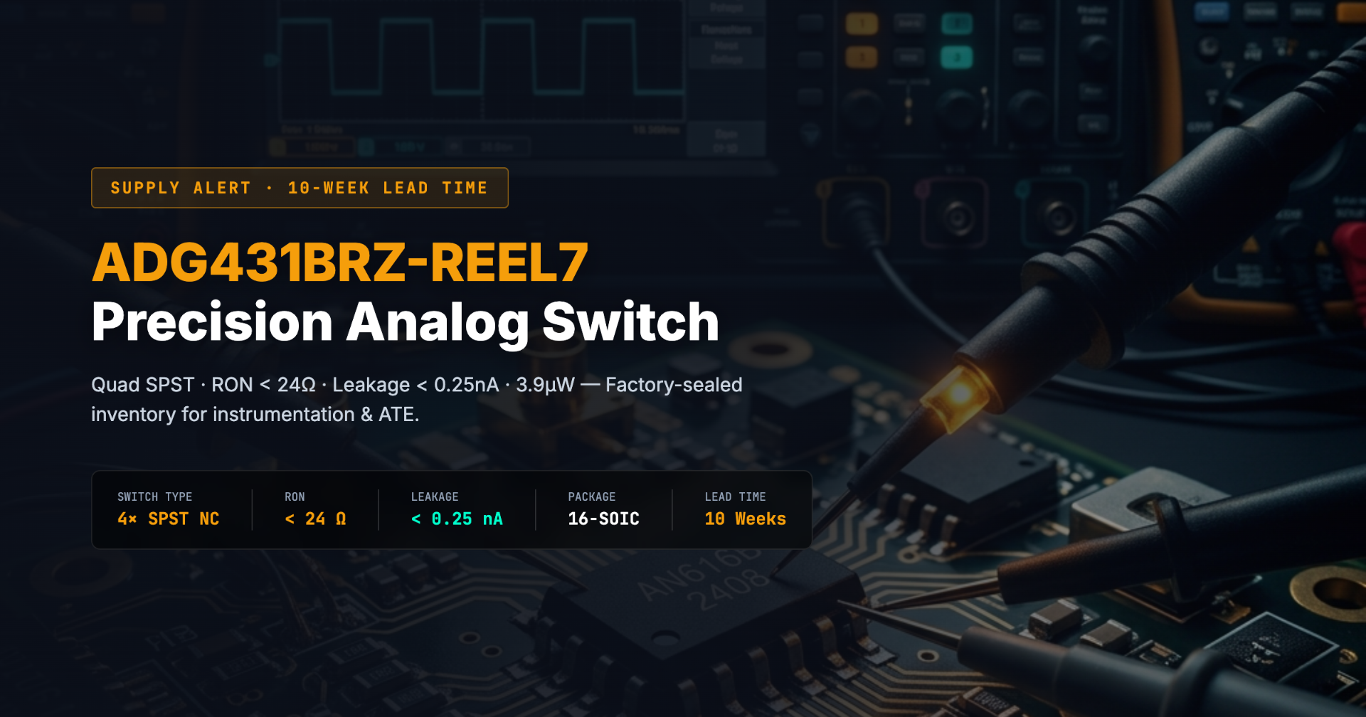
ADG431BRZ-REEL7 In Stock: ADI Precision Analog Switch — Immediate Ship
ADG431BRZ-REEL7 Supply Tightening: 10-Week Factory Lead Time Amid Rising Demand for Precision Instruments
Category: Manufacturer News & PCN/EOL | Author: Charles·Lee | Published: May 2026 | Last Updated: May 8, 2026
Key Takeaways:
- The ADG431BRZ-REEL7 is a quad SPST (normally closed) precision analog switch featuring < 24 Ω on-resistance, < 0.25 nA leakage current, and < 3.9 µW power dissipation — the gold standard for sample-and-hold circuits and multi-channel data acquisition systems.
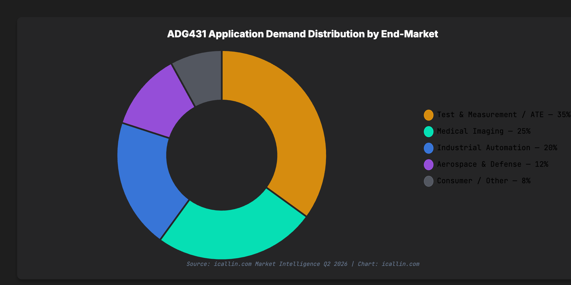
- Factory lead times have stretched to 10 weeks (up from the historical 4–6 week baseline) as ADI reallocates legacy CMOS process capacity amid surging demand from test & measurement, medical imaging, and industrial automation end markets.
- The trench-isolated variant ADG431ABRZ-REEL7 provides absolute latch-up immunity in the same 16-SOIC footprint — a pin-compatible upgrade for high-reliability applications.
- ADG431 (NC), ADG432 (NO), and ADG433 (SPDT) share the same die and package but implement different switch topologies — they are NOT drop-in interchangeable without circuit analysis.
- icallin.com maintains factory-sealed, traceable ADG431BRZ-REEL7 inventory for immediate shipment. Submit an RFQ →
Executive Summary — Why ADG431BRZ-REEL7 Lead Times Are Stretching
In the semiconductor shortage narratives that dominate trade publications, the spotlight invariably falls on GPUs, FPGAs, and power management ICs — devices with price points that make supply disruptions headline-worthy. But some of the most painful shortages happen in the unglamorous corners of the analog catalog: the $6 precision switch that holds up a $50,000 automatic test equipment rack.
The ADG431BRZ-REEL7 is precisely that kind of device. A quad SPST (Single-Pole, Single-Throw) normally closed analog switch manufactured by Analog Devices, the ADG431 has been the quiet workhorse behind precision instrumentation for over two decades. Its combination of sub-nanoamp leakage current, low charge injection, and ultralow power consumption makes it irreplaceable in sample-and-hold circuits, high-impedance sensor interfaces, and multi-channel signal routing matrices.
Now, factory lead times for the ADG431BRZ-REEL7 have stretched to approximately 10 weeks — nearly double the historical baseline of 4–6 weeks. Unit pricing in the distributor market ranges from $5.00 to $9.50 depending on volume and source, with spot-market premiums emerging for tape-and-reel quantities above 2,500 units.
The drivers are structural, not cyclical. ADI's legacy CMOS process lines — the same fabs producing the ADG431 — simultaneously serve the company's precision DAC, ADC, and analog switch product families. As demand for precision data converters surges (driven by 5G test infrastructure, next-generation medical imaging, and Industry 4.0 sensor networks), wafer starts for mature analog switches face the same capacity allocation squeeze that has plagued the broader semiconductor industry.
| Parameter | ADG431BRZ-REEL7 Snapshot |
|---|---|
| Manufacturer | Analog Devices (ADI) |
| Switch Type | Quad SPST — Normally Closed (NC) |
| On-Resistance (RON) | < 24 Ω (typ. 18 Ω) |
| Leakage Current | < 0.25 nA (typ. 0.04 nA) |
| Power Dissipation | < 3.9 µW |
| Analog Signal Range | ±15 V (VDD/VSS) |
| Charge Injection | Minimized (matched topology) |
| Switching Speed | tON 130 ns / tOFF 60 ns |
| Digital Input Compatibility | TTL / CMOS (VL supply) |
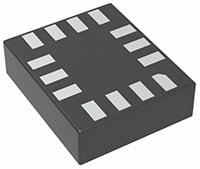
| Package | 16-SOIC (R-16A) |
| Temp Range | -40°C to +85°C (Industrial) |
| Factory Lead Time | ~10 weeks (up from 4–6 weeks) |
| Unit Price Range | $5.00 – $9.50 (qty-dependent) |
Table 1: ADG431BRZ-REEL7 Procurement Snapshot | Source: ADI Datasheet Rev. C, Market Intelligence Q2 2026 | Compiled by: icallin.com
ADG431BRZ-REEL7 Deep Specification Review — Anatomy of a Precision Analog Switch
The ADG431 may appear simple in concept — four independently controllable switches in a 16-pin SOIC — but its specifications reveal the deep analog design expertise that makes this device indispensable in precision applications.
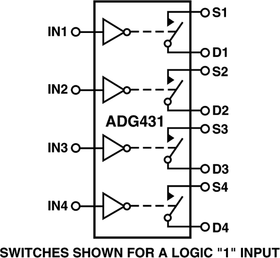
Switch Architecture: Quad SPST Normally Closed
The ADG431 contains four independent SPST analog switches, each defaulting to the normally closed (NC) state. When the corresponding digital input (IN1–IN4) is logic LOW, the switch conducts; when HIGH, the switch opens. This NC topology is critical for fail-safe designs where the signal path must remain connected in the absence of active control — common in safety-critical instrumentation and medical monitoring equipment.
The ADG432 and ADG433 variants share the same die technology but implement different topologies:
| Variant | Switch Type | Default State | Channels | Pin-Compatible? |
|---|---|---|---|---|
| ADG431 | 4× SPST | Normally Closed (NC) | 4 independent | ✅ Same pinout |
| ADG432 | 4× SPST | Normally Open (NO) | 4 independent | ✅ Same pinout |
| ADG433 | 2× SPDT | Complementary (NC/NO pairs) | 2 changeover | ✅ Same pinout |
Table 2: ADG431/ADG432/ADG433 Variant Comparison | Source: ADI Datasheet Rev. C | Compiled by: icallin.com
Critical design note: While all three variants are pin-compatible, they are not functionally interchangeable without circuit analysis. Replacing an ADG431 (NC) with an ADG432 (NO) inverts the switch logic — a channel that should be conducting at power-up will instead be open, potentially creating a signal path discontinuity that could damage downstream circuitry or corrupt measurement data.
On-Resistance: < 24 Ω with Exceptional Flatness
The ADG431's on-resistance specification of < 24 Ω (typical 18 Ω at VDD = ±15V, TA = 25°C) is competitive for a precision CMOS switch with ±15V signal capability. More importantly, the RON flatness across the full analog signal range (from VSS to VDD) is exceptionally tight — critical for maintaining signal integrity in precision measurement applications where even milliohm-level RON variation introduces gain errors.
The RON vs. temperature characteristic shows a predictable, monotonic increase from approximately 18 Ω at 25°C to approximately 35 Ω at 85°C — well within the design margin for most instrumentation applications.
Ultralow Power: < 3.9 µW
The ADG431's total power dissipation of < 3.9 µW (VDD = 12V, VSS = 0V, digital inputs at 0V or 5V) is among the lowest in the industry for a quad analog switch. The quiescent supply current is specified at < 0.1 µA for both IDD and IL — making the device suitable for battery-powered portable instruments, wireless sensor nodes, and any application where power budget is constrained.
Leakage Current: < 0.25 nA — The Specification That Matters Most
For sample-and-hold applications, the ADG431's leakage current specification is its most critical parameter. The datasheet specifies:
- IS(OFF): < 0.25 nA at 25°C — the current flowing through the source terminal when the switch is open
- ID(OFF): < 0.25 nA at 25°C — the current flowing through the drain terminal when the switch is open
- ID(ON): < 0.25 nA at 25°C — the leakage current through the drain when the switch is closed (flowing to ground, not through the signal path)
In a sample-and-hold circuit, the switch leakage directly determines the droop rate of the held voltage. With a 2,200 pF hold capacitor (as shown in the ADI reference design), the ADG431 achieves a typical droop rate of 30 µV/µs — maintaining held voltage accuracy to within 1 LSB of a 16-bit ADC for over 200 µs hold time.
Reliability and Qualification
The GeneratePdf.pdf qualification report confirms that the ADG431BRZ-REEL7 has passed the full JEDEC stress test suite:
| Stress Test | Conditions | Method | Result |
|---|---|---|---|
| HTOL (High-Temp Operating Life) | TJ ≥ 125°C, 1000 hrs | JESD22-A108 | ✅ Pass |
| HTSL (High-Temp Storage Life) | TA ≥ 150°C, 1000 hrs | JESD22-A103 | ✅ Pass |
| Temperature Cycling | -65°C to +150°C, 500 cycles | JESD22-A104 | ✅ Pass |
| THB (Temp Humidity Bias) | 85°C/85%RH, 1000 hrs | JESD22-A101 | ✅ Pass |
| Autoclave | 121°C/100%RH, 96 hrs | JESD22-A102 | ✅ Pass |
| ESD HBM | TA = 25°C | JS-001 | ✅ Pass |
| Latch-Up | Per JESD78 | JESD78 | ✅ Pass |
Table 3: ADG431BRZ-REEL7 Qualification Summary | Source: ADI Qualification Report | Compiled by: icallin.com
Market Intelligence — What's Driving ADG431 Supply Tightening
The ADG431's supply constraint reflects a broader capacity crunch in ADI's legacy CMOS analog product lines. Understanding these dynamics is essential for procurement teams planning their sourcing strategy.
Driver 1: ADI's Legacy CMOS Fab Capacity Allocation
Analog Devices manufactures the ADG431 family on mature CMOS process nodes at its internal fabrication facilities. These same process lines produce the company's precision DAC, ADC, and voltage reference product families — all of which are experiencing elevated demand driven by 5G test infrastructure buildout and industrial IoT expansion. Unlike leading-edge digital fabs where capacity can be rapidly expanded, legacy analog fabs operate on fixed wafer-start schedules with limited flexibility to increase output.
Driver 2: Test & Measurement Platform Refresh
The global ATE (Automatic Test Equipment) industry is in the midst of a multi-year platform refresh cycle. Next-generation SoC test systems — designed to characterize 5G RF front-ends, automotive ADAS processors, and AI accelerators — require dense arrays of precision analog switches for signal routing and relay replacement. A single ATE pin electronics card may consume 16–64 ADG431-class switches, and a complete test system comprises hundreds of such cards. The aggregate demand from the ATE refresh cycle alone represents a significant share of ADG431 production volume.
Driver 3: Medical Imaging Demand
Multi-channel signal routing is fundamental to modern medical imaging systems. CT scanners, MRI systems, and ultrasound platforms all require precision analog switches for transducer array multiplexing, signal conditioning path selection, and calibration circuit switching. The ADG431's sub-nanoamp leakage and low charge injection make it particularly well-suited for the high-impedance, noise-sensitive front-end circuits in these systems. As healthcare infrastructure investment accelerates globally — particularly in Asia-Pacific — medical imaging demand for precision analog switches continues to grow.
Driver 4: Industrial 4.0 Sensor Multiplexing
The proliferation of sensor networks in smart factories, process control systems, and predictive maintenance platforms drives demand for multi-channel data acquisition systems. PLCs and DCS controllers increasingly embed precision analog multiplexers and switches for thermocouple scanning, strain gauge conditioning, and vibration sensor readout. The ADG431's ultralow power consumption makes it particularly attractive for distributed sensor nodes powered by energy harvesting or limited battery budgets.
Supply Chain Risk Assessment
The convergence of these four demand drivers creates a compounding effect on ADG431 availability. Unlike high-profile shortages (GPUs, HBM, advanced FPGAs) that attract media attention and management visibility, the ADG431's low unit price and perceived commodity status means that supply disruptions often go undetected until the production line stops. Procurement teams accustomed to treating analog switches as "always available" catalog parts are discovering that legacy CMOS capacity is finite, and the competition for that capacity is intensifying across all end markets simultaneously.
The risk is further amplified by the ADG431's limited second-source ecosystem. While Vishay's DG411 family offers functional equivalence, the package differences (DIP-16 vs. SOIC-16) and subtle parametric variations (RON, leakage, charge injection) mean that true drop-in substitution requires engineering validation — adding weeks to the mitigation timeline. For production lines with frozen BOMs and qualification-locked designs, the ADG431BRZ-REEL7 is effectively sole-sourced.
| Risk Factor | Severity | Trend | Mitigation |
|---|---|---|---|
| ADI legacy CMOS capacity allocation | 🔴 High | Worsening | Secure verified spot inventory immediately |
| ATE platform refresh demand surge | 🟡 Medium | Stable-High | Lock multi-quarter allocations with distributors |
| Medical imaging infrastructure growth | 🟡 Medium | Growing | Diversify across ADG431/ADG431A variants |
| Industrial IoT sensor deployment | 🟢 Low-Medium | Growing | Evaluate ADG408 MUX for channel consolidation |
| Limited cross-brand second-sourcing | 🔴 High | Stable | Qualify Vishay DG411 as emergency alternative |
| Counterfeit risk at low price point | 🟢 Low | Stable | Purchase from verified sources with COC |
Table 6: ADG431BRZ-REEL7 Supply Chain Risk Matrix | Source: icallin.com Market Intelligence | Compiled by: icallin.com
Application Deep Dive — Where ADG431 Delivers Irreplaceable Value
Sample-and-Hold Circuits
The ADG431's primary application stronghold is in precision sample-and-hold (S/H) circuits. The ADI reference design (Figure 2 in the datasheet) demonstrates a fast, accurate S/H implementation achieving:
- Acquisition time: 850 ns (to 0.01% settling)
- Droop rate: 30 µV/µs (with 2,200 pF polystyrene hold capacitor)
- Pedestal error: < 5 mV over ±10V input range (with charge injection compensation network)
The key to this performance is the ADG431's combination of low leakage current (< 0.25 nA) and minimized charge injection. The reference design includes a second switch (SW2) operating in parallel with the primary switch (SW1) to create a differential charge injection cancellation — a technique that exploits the ADG431's matched switch characteristics to reduce pedestal error by up to 10×.
Multi-Channel Data Acquisition Systems
In 16+ channel data acquisition architectures, the ADG431's four independent SPST switches serve as programmable signal routing elements. By cascading multiple ADG431 devices, designers build flexible MUX trees that can connect any combination of input channels to shared instrumentation amplifiers or ADCs. The break-before-make switching characteristic prevents signal shorting during channel transitions, protecting both the source circuits and the measurement chain.
Automatic Test Equipment (ATE)
The ATE industry has increasingly adopted CMOS analog switches as alternatives to mechanical relays in signal routing matrices. The ADG431 offers several advantages over electromechanical relays:
- Switching speed: 130 ns turn-on vs. 1–5 ms for mechanical relays (1,000× faster)
- Lifetime: Essentially unlimited switching cycles vs. 10⁶–10⁸ for mechanical relays
- Size: 16-SOIC vs. bulky relay packages — enabling higher channel density per card
- Power: 3.9 µW vs. 100–500 mW coil power for latching relays
Medical Imaging Front-Ends
In ultrasound systems, the ADG431 routes signals between transducer elements and the receive beamformer. The sub-nanoamp leakage ensures that charge stored on the transducer's parasitic capacitance is not drained during the receive window, preserving signal-to-noise ratio. In CT scanner detector arrays, multiple ADG431 devices multiplex signals from hundreds of scintillator-photodiode channels to shared digitization circuits.
| Application | Key ADG431 Spec | Performance Impact | Alternative Impact (if unavailable) |
|---|---|---|---|
| Sample-and-Hold | Leakage < 0.25 nA | Droop rate 30 µV/µs | 10× higher droop with generic CMOS switch |
| Multi-Channel DAQ | 4× independent SPST | Flexible N:1 MUX topology | Requires multiple single-channel devices |
| ATE Signal Routing | tON 130 ns, unlimited cycles | 1,000× faster than relays | Mechanical relay: size/power/lifetime penalty |
| Medical Imaging | Low charge injection | < 5 mV pedestal error | Corrupted receive signal, reduced SNR |
Table 4: Application-Specific ADG431 Performance Matrix | Source: ADI Datasheet Rev. C & Application Notes | Compiled by: icallin.com
ADG431 Family & Cross-Brand Migration Guide
When the ADG431BRZ-REEL7 is unavailable or lead times are unacceptable, procurement teams need to understand the available alternatives — both within ADI's product family and from competing manufacturers.
ADG431 vs ADG431A: Trench Isolation
The ADG431ABRZ-REEL7 adds trench isolation between the NMOS and PMOS transistors of each CMOS switch. In junction-isolated designs (standard ADG431), parasitic PNPN structures can form silicon-controlled rectifier (SCR) paths that, under overvoltage conditions, lead to latch-up — a potentially destructive condition where the device draws excessive current. Trench isolation physically eliminates these parasitic junctions by inserting an insulating oxide barrier, resulting in a completely latch-up proof switch. The ADG431A is pin-compatible with the ADG431 and should be specified for any application where input overvoltage transients are possible.
Cross-Brand Alternatives
For multi-sourcing strategies, several competing devices offer functional equivalence:
- Vishay DG411DJ-E3: Quad SPST analog switch with < 30 Ω RON and ±15V signal range. DIP-16 package (not SOIC) — requires footprint adaptation. Vishay-qualified supply chain provides true multi-sourcing capability.
- ADG419BRZ: Single-channel SPDT (changeover) switch with < 25 Ω RON. Different topology (SPDT vs SPST) — suitable for applications requiring signal path selection rather than on/off switching.
- ADG408BN: 8:1 analog multiplexer with < 80 Ω RON. Higher RON but consolidates 8 channels into a single device — reducing component count in multi-channel systems.
| Priority | Part Number | Type | RON | Leakage | Package | Advantage |
|---|---|---|---|---|---|---|
| 🟢 Primary | ADG431BRZ-REEL7 | 4× SPST NC | < 24 Ω | < 0.25 nA | 16-SOIC | Hot Stock — Immediate Ship |
| 🟢 Upgrade | ADG431ABRZ-REEL7 | 4× SPST NC | < 24 Ω | < 0.25 nA | 16-SOIC | Trench-isolated, latch-up proof |
| 🟡 SPDT | ADG419BRZ | 1× SPDT | < 25 Ω | < 0.5 nA | 8-SOIC | Changeover topology |
| 🟡 MUX | ADG408BN | 8:1 MUX | < 80 Ω | < 1 nA | DIP-16 | 8 channels per device |
| 🟡 Cross-Brand | DG411DJ-E3 | 4× SPST | < 30 Ω | < 0.5 nA | DIP-16 | Vishay multi-source |
Table 5: 5-Model Verified Procurement Matrix for Precision Analog Switches | Compiled by: icallin.com

Frequently Asked Questions
Q1: What is the current factory lead time for ADG431BRZ-REEL7?
As of Q2 2026, the factory lead time for ADG431BRZ-REEL7 through ADI's authorized distribution network is approximately 10 weeks, up from the historical 4–6 week baseline. This extension is driven by capacity allocation constraints on ADI's legacy CMOS process lines, which serve multiple product families simultaneously. Purchasing from verified independent distributors like icallin.com with existing spot inventory is the most effective strategy to bypass this queue.
Q2: What is the difference between ADG431 and ADG431A (trench-isolated version)?
The ADG431ABRZ-REEL7 is functionally identical to the ADG431 but uses trench isolation instead of junction isolation between the NMOS and PMOS transistors. This eliminates parasitic SCR latch-up paths, making the ADG431A completely latch-up proof. The ADG431A is pin-compatible and should be specified for applications where input signals may exceed the supply rails during transient events, or where high-reliability qualification demands latch-up immunity.
Q3: Can I use ADG432 or ADG433 as a drop-in replacement for ADG431?
Functionally, no. While all three variants are pin-compatible (same 16-SOIC footprint and pinout), they implement different switch topologies. The ADG431 is normally closed (NC) — conducting when the control input is LOW. The ADG432 is normally open (NO) — conducting when HIGH. The ADG433 provides two SPDT changeover switches. Substituting an ADG432 for an ADG431 inverts the control logic, which can cause signal path discontinuities, incorrect measurements, or downstream circuit damage. Always verify your circuit's logic polarity requirements before substituting.
Q4: What is the maximum analog signal voltage that ADG431 can handle?
The ADG431 can handle analog signals across the full supply range from VSS to VDD. With the recommended ±15V dual supply configuration, this means the analog signal can swing from -15V to +15V (30Vpp). For single-supply operation with VDD = 12V and VSS = 0V, the analog range is 0V to 12V. The absolute maximum rating for VDD to VSS is 44V, allowing supply configurations up to ±22V for extended dynamic range applications.
Q5: How does the ADG431's charge injection compare to competing analog switches?
The ADG431's charge injection is minimized through a matched switch topology that creates differential cancellation. In the ADI reference S/H design (with the RC/CC compensation network), pedestal error is reduced to < 5 mV over the full ±10V input range. This is competitive with the best precision analog switches in the market. For comparison, generic CMOS switches (such as the CD4066B) can exhibit 10–50× higher charge injection, resulting in unacceptable pedestal errors for 14-bit and higher resolution systems.
Q6: Is the ADG431BRZ-REEL7 qualified for automotive or military applications?
The ADG431BRZ-REEL7 is qualified for industrial temperature range (-40°C to +85°C) per the JEDEC stress test suite documented in ADI's qualification report (HTOL, HTSL, TC, THB, Autoclave, ESD HBM/CDM, Latch-Up — all pass). However, it does not carry AEC-Q100 automotive qualification or MIL-PRF-38535 military screening. For automotive applications, contact ADI for potential custom qualification programs. For military/aerospace, ADI offers selected analog switch products through their defense product line — consult your ADI sales representative for availability.
Conclusion
The ADG431BRZ-REEL7 is a quiet giant of the analog semiconductor world. It does not command the attention of high-speed FPGAs or the price points of power management ICs, but its absence stops production lines. The sub-nanoamp leakage, ultralow power consumption, and minimized charge injection that define this device are not specifications that can be compromised without measurable degradation in measurement accuracy, signal integrity, and system reliability.
With 10-week factory lead times compressing procurement windows across the test & measurement, medical imaging, and industrial automation sectors, proactive inventory management is no longer optional — it is a production continuity imperative. The ADG431 family's pin-compatible variant structure (ADG431/431A/432/433) provides flexibility, but only for teams that understand the functional differences between NC, NO, and SPDT topologies.
icallin.com maintains factory-sealed, fully traceable ADG431BRZ-REEL7 inventory for immediate shipment — with Certificate of Conformance, lot/date code documentation, and REACH compliance verification available on request.
📧 Submit an RFQ for ADG431BRZ-REEL7 and ADI Precision Analog Switch Family →
Related Internal Resources
- ADG431BRZ-REEL7 — Product Detail
- Analog Devices Manufacturer Page
- Analog Switch Category
- Submit RFQ
- Hot Products
*Charles·Lee is a Senior Analog Applications Engineer and Supply Chain Strategist at icallin.com, specializing in precision signal chain architecture, analog switch selection, and high-reliability component procurement for instrumentation and medical markets. With over 12 years of experience bridging the gap between analog design teams and procurement organizations, Charles helps OEMs secure critical components in allocation-constrained markets.

Top Recommended part