How Printed Circuit Boards Work: Structure and Design
How Printed Circuit Boards Work: Structure, Function, and Design Flow
Open almost any electronic product and you will find a printed circuit board holding the parts together and giving them defined electrical paths. The board may be smaller than a coin or large enough to fill an equipment rack, yet its basic job is the same: support components, connect them according to a circuit, and turn an electrical design into something that can be assembled repeatedly.
Understanding a PCB is easier when it is viewed as a coordinated structure rather than a flat green sheet. The insulating base, copper conductors, pads, protective coating, printed markings, and mounted components all perform different tasks. Their arrangement is established through a design process that begins with a schematic and ends with manufacturable production data.
Why PCBs Matter in Modern Electronics
Before printed circuit boards became the standard platform for electronics, many connections were made with individual wires or point-to-point construction. That approach can still be useful for a simple prototype, but it becomes difficult to control as the number of parts and connections increases. A PCB converts those connections into a repeatable geometric pattern.
They Bring Complex Functions Into One Assembly
A modern circuit may combine processors, memory, sensors, power conversion, communications, connectors, and protection components. The PCB gives every part a physical location and connects the required pins through copper tracks, planes, pads, and vias. Multilayer construction adds routing space inside the board, allowing more functions to fit within a practical outline.
The board does not create those functions by itself. Performance still depends on the selected components and the electrical design. Its value is that it provides an organized platform on which the complete system can be built.
They Help Control Electrical Performance
Placement and routing influence how current and signals travel. Trace geometry affects resistance and, for controlled-impedance connections, the relationship between a trace and its reference plane. Return-path continuity, separation between sensitive and noisy circuits, and power-distribution geometry can all influence interference and signal quality.
A PCB therefore does more than replace loose wire. It gives the designer control over conductor location, spacing, layer assignment, and the relationship between connected parts. Good layout supports predictable behavior; poor layout can undermine an otherwise correct schematic.
They Support Repeatable Production
Once the board outline, copper artwork, drilled holes, mask openings, and markings are defined, the same design data can be used to build multiple boards. Component locations can also be communicated through placement files and assembly drawings. This repeatability reduces the variation that would arise if every unit were wired manually.
Repeatability is not the same as guaranteed quality. The design still needs review, the selected manufacturing process must be capable of producing it, and the finished assembly must be inspected and tested. The PCB provides the controlled foundation for those activities.
They Make Better Use of Space
Connections do not all need to occupy the outer surfaces. Internal copper layers can carry signals, ground, and power, while both sides may hold components when the assembly process permits. This three-dimensional use of the board helps electronic products become smaller without turning every connection into a fragile wire link.
More layers are not automatically better. They add routing options but also affect stackup planning, fabrication complexity, cost, and inspection. Layer count should follow circuit density and electrical requirements rather than being treated as a performance score.
The Main Parts of a Printed Circuit Board
A finished assembly is often called a PCBA, while the unpopulated board is the PCB. The distinction is useful because some elements belong to the board construction and others are mounted later during assembly.
| Element | Primary role | Design concern |
|---|---|---|
| Substrate or laminate | Mechanical support and electrical insulation | Material properties, thickness, heat, moisture, and rigidity |
| Copper traces and planes | Conductive paths for signals, power, and ground | Width, spacing, thickness, impedance, and current |
| Pads | Solderable connection points for component leads or terminals | Footprint accuracy, solderability, and thermal behavior |
| Vias | Connections between copper layers | Drill geometry, plating, current, and reliability |
| Solder mask | Protective coating over most exposed copper | Openings, clearances, adhesion, and imaging capability |
| Silkscreen or legend | Human-readable component and assembly information | Readability, polarity, orientation, and component clearance |
| Components | Provide the circuit's active and passive functions | Correct part, orientation, package, placement, and assembly method |
Substrate and Laminate
The substrate is the insulating body that gives the board its shape and supports the copper. Glass-reinforced epoxy materials in the FR-4 family are common in rigid boards because they combine electrical insulation, mechanical strength, broad availability, and established processing. Other constructions are used when a product needs flexibility, lower high-frequency loss, better heat transfer, or a different mechanical behavior.
Material selection cannot be reduced to color or a generic family name. The exact laminate influences dielectric behavior, thermal expansion, moisture response, thickness tolerance, and the stresses seen by plated holes. Those properties become more important as frequency, layer count, operating temperature, or reliability requirements increase.
Copper Traces, Planes, Pads, and Vias
Copper forms the electrical network. Narrow or wide traces connect individual nodes, larger regions can distribute power or provide a ground reference, and pads create soldering surfaces for component terminals. Vias are plated holes or microstructures that carry a connection from one copper layer to another.
Every copper feature has a physical shape. A trace that is too narrow for its current may develop excessive temperature rise. A reference plane broken by a slot may force return current to take a longer route. A pad copied from the wrong package may look plausible on screen but fail during assembly. Electrical connectivity is necessary, yet geometry determines whether that connectivity works in the finished product.
Mounted Electronic Components
Integrated circuits, resistors, capacitors, inductors, transistors, diodes, connectors, and many other parts are attached to the board. Some use surface-mount packages placed on pads; others have leads inserted through holes. Mixed assemblies may use both methods.
Each component contributes a specific function, but the ordering code matters. Parts with similar names can have different packages, pinouts, temperature grades, or electrical limits. The footprint and orientation marks must match the exact component selected for production.
Solder Mask and Silkscreen
Solder mask covers most of the external copper while leaving intended pads and contacts exposed. It helps reduce accidental solder bridging and protects conductors from routine handling and contamination. It does not make the board waterproof, nor does it replace the spacing required for electrical safety.
Silkscreen, also called the legend, provides reference designators, connector names, polarity symbols, pin-one marks, revision information, and other instructions for assembly or service. Clear markings prevent mistakes only when they remain visible after components are installed.

How the Layers Work Together
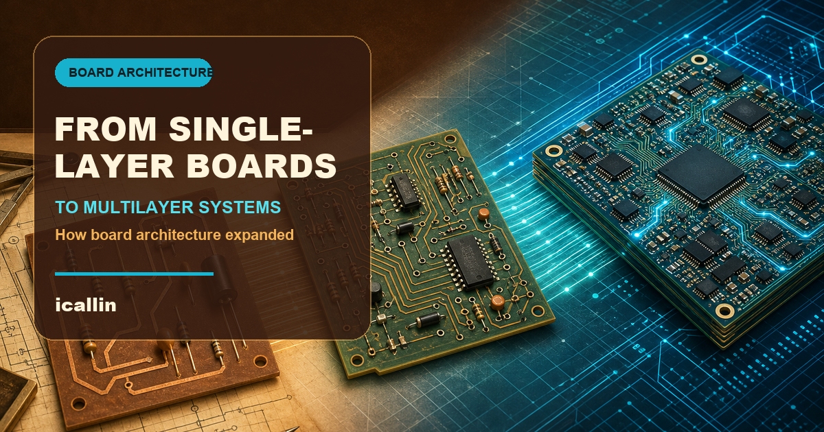
A single-sided board has conductive artwork on one side of an insulating base. A double-sided board provides copper on both sides and can use plated through-holes to connect them. A multilayer board laminates additional copper and dielectric layers inside the structure.
The correct construction depends on what must be routed and how the circuit behaves. A simple low-density design may fit comfortably on two layers. A dense controller or high-speed interface may benefit from nearby ground references, dedicated power distribution, and more routing channels. The stackup defines the order and spacing of these layers, so it should be settled before critical traces are finalized.
The visual appearance of a board reveals little about its internal organization. Two assemblies with similar outlines may have very different layer counts, copper weights, materials, and reliability limits. The fabrication drawing and approved stackup are the authoritative descriptions.
From Circuit Idea to a Manufacturable PCB
The design process converts an electrical concept into a controlled set of physical instructions. Four activities form the core of that transition.
1. Capture the Schematic
The schematic records the intended electrical relationships among components. Symbols represent parts, while nets show which pins must connect. Power rails, ground domains, interfaces, protection devices, and test points are defined here before their physical positions are chosen.
A clean schematic makes later review easier. Consistent net names, component values, part references, and connector labels help the layout designer understand circuit intent. Electrical-rule checking can reveal certain missing or conflicting connections, but it cannot prove that every design decision is correct.
2. Build the Physical Layout
During layout, the board outline is created, footprints are placed, and connections are routed through traces, planes, and vias. Mechanical restrictions from the enclosure, connectors, mounting hardware, keepout zones, and component height must be respected alongside the electrical requirements.
Placement normally comes before detailed routing because short, direct connections begin with sensible component relationships. Power stages, clocks, high-speed links, analog inputs, antennas, and heat-generating parts may each need different treatment. The layout is therefore a physical interpretation of the schematic, not an automatic drawing exercise.
3. Review Manufacturability
Design for manufacturability, or DFM, asks whether the intended board can be fabricated and assembled with the selected process. Trace width and clearance, drilled-hole size, annular ring, solder-mask dams, copper-to-edge spacing, board outline details, and panel considerations all need to fit current process limits.
Assembly adds another set of questions: Can solder paste be printed consistently? Are polarized parts clearly marked? Can inspection equipment see critical joints? Is there access for test and rework? Solving these issues in layout is usually easier than correcting them after hardware exists.
4. Run Rule Checks and Inspect the Output
A design-rule check, or DRC, compares layout geometry with configured constraints. It can find clearance violations, unconnected nets, drill problems, and other defined errors. The result is only as good as the rules entered, so a clean DRC report does not replace engineering review.
Before release, fabrication and assembly outputs should be inspected independently. Check the outline, copper, mask, legend, drill data, component positions, orientations, and revision identifiers. Confirm that the exported files represent the intended version and that no layer was mirrored, omitted, or scaled.
A Practical Release Checklist
- Confirm the schematic and bill of materials use the intended component ordering codes.
- Verify every footprint against the relevant package drawing.
- Check the board outline, mounting points, connectors, and enclosure clearances.
- Review power paths, return paths, sensitive signals, and high-current geometry.
- Run electrical and design-rule checks with project-specific constraints.
- Inspect fabrication and drill data in an independent viewer.
- Review assembly drawings, polarity marks, pin-one indicators, and test access.
- Record the revision so the physical board can be traced to its source files.
Frequently Asked Questions
What is the simplest definition of a PCB?
A PCB is an insulating structure carrying patterned copper conductors and connection points for electronic components. It provides both physical support and repeatable electrical interconnection.
What is the difference between a PCB and a PCBA?
PCB usually refers to the bare printed circuit board. PCBA refers to the assembled board after components have been soldered or otherwise attached.
Why are many rigid circuit boards made from FR-4?
FR-4 materials offer a practical combination of insulation, strength, process maturity, availability, and cost. The exact grade still needs to meet the product's thermal, electrical, mechanical, and environmental requirements.
Does a multilayer PCB always perform better than a two-layer board?
No. Extra layers can provide more routing space and closer reference planes, but the benefit depends on a correctly planned stackup and layout. A simple circuit may gain nothing from unnecessary layers.
Is passing DRC enough to release a board for production?
No. DRC finds violations of configured geometric rules. Engineers must also verify circuit intent, footprints, component choices, mechanical fit, stackup, manufacturability, assembly information, and exported files.
Conclusion
A printed circuit board turns a schematic into a physical, repeatable electronic assembly. The substrate provides support and insulation; copper creates the conductive network; pads and vias join components and layers; solder mask protects exposed circuitry; and the legend guides people who build or service the product.
Those elements work only when the design process connects electrical intent with physical reality. Schematic capture defines the circuit, layout organizes it, DFM aligns it with production capabilities, and rule checks help expose mistakes. Understanding that full chain is the foundation for evaluating any PCB, from a basic two-layer controller to a dense multilayer system.