Part No:
STB6N52K3
Category:
Transistors
Description:
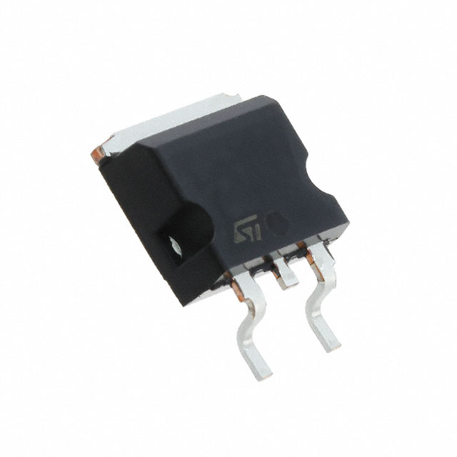
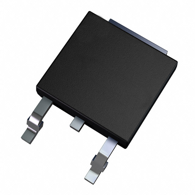
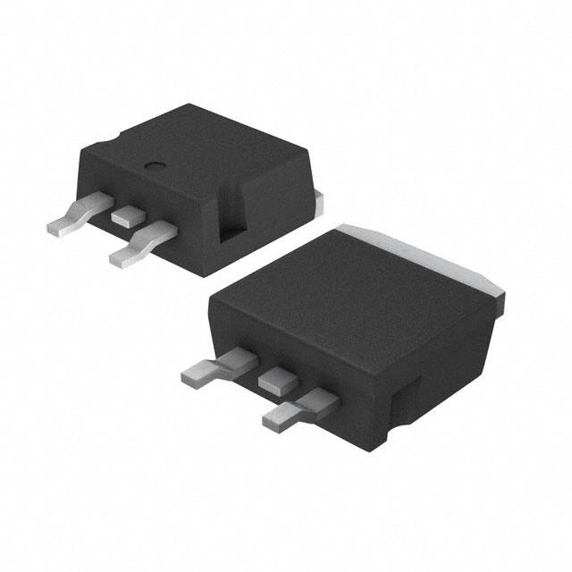
MOSFET (Metal Oxide) N-Channel Tape & Reel (TR) 1.2 ? @ 2.5A, 10V ±30V 670pF @ 50V 26nC @ 10V TO-263-3, D2Pak (2 Leads + Tab), TO-263AB
Package:
-
Production Status:
In Stock Status:
Specification
Package / Case
TO-263-3, D2Pak (2 Leads + Tab), TO-263AB
Transistor Element Material
Moisture Sensitivity Level (MSL)
Terminal Finish
Matte Tin (Sn) - annealed
Peak Reflow Temperature (Cel)
Time@Peak Reflow Temperature-Max (s)
Configuration
SINGLE WITH BUILT-IN DIODE
Input Capacitance (Ciss) (Max) @ Vds
Current - Continuous Drain (Id) @ 25°C
Gate Charge (Qg) (Max) @ Vgs
Drive Voltage (Max Rds On,Min Rds On)
Continuous Drain Current (ID)
Gate to Source Voltage (Vgs)
Drain Current-Max (Abs) (ID)
Drain to Source Breakdown Voltage
Pulsed Drain Current-Max (IDM)
Avalanche Energy Rating (Eas)
Products Detail
STB6N52K3 Overview
As a result of avalanche breakdown, energy applied to the MOSFET is called avalanche energy, and the avalanche energy rating is 110 mJ.A device's maximum input capacitance is 670pF @ 50V, but its input capacitance parameter, CI, is measured as the capacitance between the input terminals of the device with either input grounded.Its continuous drain current is 5A for this device. Drain current refers to the capacity of the device to conduct continuous current.Single MOSFETs transistor is the voltage at which VDS flows at a specified ID value, wSingle MOSFETs transistorh VGS=525V, and this device has a drain-to-source breakdown voltage of 525V voltage.Its drain current is 5A, and it is the maximum continuous current the device can conduct.A device's turn-off delay time is the amount of time it takes to charge its input capacitance before drain current conduction can begin, which is 31 ns.Its maximum pulsed drain current is 20A, which is also its maximum rating peak drainage current.Before drain current conduction begins, the device's input capacitance must be charged, so the delay time is 10 ns.Generally, the gate-source voltage (VGS) of a FET transistor is the voltage across its gate-source terminal, which is 30V.This device uses no drive voltage (10V) to reduce its overall power consumption.
STB6N52K3 Features
the avalanche energy rating (Eas) is 110 mJ
a continuous drain current (ID) of 5A
a drain-to-source breakdown voltage of 525V voltage
the turn-off delay time is 31 ns
based on its rated peak drain current 20A.
STB6N52K3 Applications
There are a lot of STMicroelectronics
STB6N52K3 applications of single MOSFETs transistors.
- Power Tools
- Motor Drives and Uninterruptible Power Supples
- Synchronous Rectification
- Battery Protection Circuit
- Telecom 1 Sever Power Supplies
- Industrial Power Supplies
- PFC stages, hard switching PWM stages and resonant switching
- PWM stages for e.g. PC Silverbox, Adapter, LCD & PDP TV,
- Lighting, Server, Telecom and UPS.
- DC-to-DC converters
Key Features
No key features available
Application scenarios
No application scenarios available
Documents