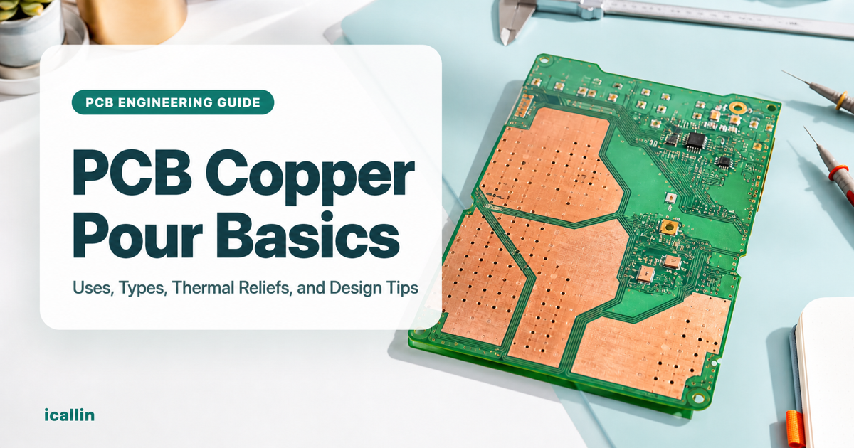
PCB Panelization: Assembly Yield and Depaneling Guide
PCB Panelization: Optimize for Good Boards, Not Just More
PCB panelization should minimize the cost of usable assemblies, not merely maximize the number of outlines inside a rectangle. A successful panel fits the fabrication and assembly processes, stays adequately supported, provides reliable alignment and separates without damaging the product.
An extra row of boards is valuable only if those boards survive printing, placement, reflow, testing and depaneling. That is the difference between efficient nesting and production-ready panel design.
Separate the fabrication panel from the assembly panel
The fabrication panel is the larger manufacturing format used to process the bare boards. The assembly panel is the array delivered or prepared for component assembly. They may be related, but they are not necessarily identical.
Ask who owns each layout and when approval is required. A fabricator can optimize its working panel while the assembler needs a smaller array with particular rails, fiducials and support locations. A panel that suits one machine may not fit the next.
Start with the board outline, component overhangs, finished thickness, layer construction and production quantity. Add the assembly line's dimensional and handling requirements before exploring how many copies fit.
Choose the separation method around the product
V-scoring is useful for suitable straight-line boundaries. Routed separation leaves channels around the outlines and tabs that retain each board until removal. Irregular shapes and edge features often make routing more flexible, but the final stress depends on the tab design, cutting equipment and support—not the method name alone.
Eurocircuits documents these as distinct panel options with different constraints. Its numerical limits describe its own service, not universal rules for all factories. Use the same principle when discussing another supplier's capabilities. Panel construction and separation guidance.
Rails are supporting features, not a third separation process. They provide handling space and locations for alignment marks, tooling or identification. Their width and necessity depend on the selected process. They also occupy material and can affect cost.

Review the panel as an assembly fixture
A useful panel remains stable where the process applies force or heat. Evaluate how it is held during paste printing, supported beneath component placement and handled through reflow. Thin boards or long unsupported spans may need additional consideration even when the outline fits comfortably.
Fiducials provide optical reference information; tooling holes serve a different mechanical role. Agree their locations and clearances with the assembler. Do not assume a board-level mark can replace a panel-level datum in every process.
Keep component overhangs visible in the panel drawing. A connector extending past one board edge may collide with its neighbor or the separation tool. Include bottom-side parts and nozzle access, not only the top-side placement image.
Mixed-design panels can be practical when the boards share a compatible construction and their production ratios make sense. Otherwise, one slow-moving design can leave unused partners. Rotation may improve nesting, but check its consequences for assembly programming, handling and thermal behavior.
Design for the moment the boards are separated
The product is most vulnerable when support changes and the panel is cut or broken apart. Put separation lines, tab positions and the intended removal method into the design review before placing sensitive components near the edge.
Ceramic capacitors deserve particular attention. Murata notes that board bending can crack mounted capacitors and recommends placement that reduces stress near board breaks. This is a component-layout constraint, not something a clean-looking edge proves acceptable. Murata guidance on board bending.
Ask for process-specific copper and component clearances. Avoid copying a single clearance number from another panel technology. Review how each board is supported during the cut, where any remaining tab protrusion will sit, and whether the final enclosure tolerates that edge condition.
A small pilot run should include separation and inspection of the actual assembled panel. A bare-board trial cannot reveal every failure mode of a populated assembly.
Compare good-board cost with an explicit example
Consider two hypothetical layouts. Panel A costs $24 to process and contains eight boards; assume its combined assembly-and-separation yield is 99%. Panel B costs $28 and contains ten boards, but assume a 92% yield. Under those simplified assumptions:
- A produces 7.92 expected good boards per panel: $24 / 7.92 ≈ $3.03 each.
- B produces 9.20 expected good boards per panel: $28 / 9.20 ≈ $3.04 each.
The denser arrangement is not cheaper per good board in this example. These figures are invented for calculation, not market prices or measured yields. A real comparison must also account for component value, inspection, rework, scrap and equipment cycle time.
Panelization reduces repeated handling, but placement time still depends on how many components the machine installs. A sixteen-up panel does not automatically make the entire assembly line sixteen times faster.
Release one coordinated panel package
The approved package should connect the single-board revision to the panel drawing, array positions, orientation, rail features and depaneling instructions. Stencil, placement, inspection and test data must describe the same arrangement.
Track defects by panel position when investigating repeated problems. A pattern concentrated at one edge may tell a different story from failures associated with one component across all positions. Sharing a panel does not guarantee every position experiences identical plating or thermal conditions.
Good panelization is a compromise among material use, handling, assembly access and separation. Optimize that complete route instead of chasing the largest count on a screenshot.
FAQ
Is V-scoring always cheaper than routed tabs?
No. It can simplify separation for suitable geometry, but total cost depends on handling, clearances, support, tooling and yield. Compare the complete production process for the actual board.
Can different PCB designs share an assembly panel?
Yes, when their construction, assembly process and production ratios are compatible. Confirm the arrangement with both the fabricator and assembler before releasing coordinated manufacturing data.
Share Your PCB Panel Requirements
Send icallin your PCB manufacturing or PCBA assembly requirements, including the single-board data and any approved panel or depaneling instructions.