In Stock: W25Q128JVSIQ (QE Bit) & NTMFS5C430NLT1G (200A)
In Stock Now: Taming the W25Q128JVSIQ (QE Boot Loop) & NTMFS5C430NLT1G (VRM Ringing)
Category: Hot Stock & Featured Parts | Author: Charles·Lee | Published: March 31, 2026 | Last Updated: March 31, 2026

[!CAUTION]
Engineering Alert (Q2 2026): Finding components in stock is only half the battle. If you procure the highly allocated Winbond W25Q128JVSIQ without understanding its "Q" suffix, your IoT gateway bootloaders will infinitely trap in a lock cycle. If you place the onsemi NTMFS5C430NLT1G into an AI Server VRM without calculating its ultra-fast $dv/dt$ overshoot, 200 Amps of current will generate catastrophic switch-node ringing and incinerate your MOSFETs.
As contract manufacturers (CMs) finalize their Bill of Materials (BOM) for Q2 production runs, securing reliable inventory for high-mix, high-volume products is paramount. We are currently witnessing a massive dichotomy in the semiconductor market: while top-tier fabs aggressively pivot their manufacturing lines toward high-bandwidth memory (HBM3e) and advanced GPU nodes, legacy component packages and discrete power stages are being starved of test-and-assembly capacity.
However, intelligent tracking of Product Change Notifications (PCNs) and profound electrical knowledge of the parts can turn this crisis into a tactical advantage.
In this exhaustive 4,000-word engineering masterclass, we will deconstruct Winbond's pivotal capacity PCN (MM202510-02-A), diagnose the root cause of the W25Q Quad Enable (QE) boot-loop disaster in U-Boot systems, and perform the brutal RC Snubber mathematics required to safely deploy the 1.4 mΩ onsemi NTMFS5C430NLT1G inside 200A AI Server power supplies.
Both of these ultra-critical components are currently in stock and continuously replenished at icallin.com. Let's dig into the engineering mechanics.
1. Winbond PCN MM202510-02-A: Why PTI Testing Capacity Matters
Millions of IoT edge devices, consumer routers, and embedded Linux microcontrollers (like Xilinx Zynq or ESP32) rely on a single, ubiquitous component to house their bootloader code: the 128M-bit (16M-byte) SPI NOR Flash.
SOP8 208-mil vs. The DDR5 Tsunami: A Foundational Conflict
As global semiconductor memory foundries like Micron, Samsung, and SK Hynix dedicate their entire backend packaging and testing (OSAT) floors exclusively to lucrative DDR5 memory modules and AI High-Bandwidth Memory (HBM), the supply chain for legacy "dumb" storage like SPI NOR Flash is collapsing. Many hardware designers feared that legacy SOP8 (208-mil) packages would face imminent End-of-Life (EOL) or catastrophic 52-week lead times by late 2026.
PTI Expansion Secures Q2-Q4 2026 Router/Gateway Production
Winbond, understanding its dominance in the embedded router market, pushed back. On October 13, 2025, Winbond officially stabilized the market by issuing Product Change Notification Z200-PCN-MM202510-02-A.
This document, flagged as a "Major Change" due to the introduction of a new facility, officially added Powertech Technology Inc. (PTI) as an additional Final Test (FT) site specifically for the SOP8 208-mil product line. Winbond formally initiated this capacity increase in January 2026.
What does this translate to on the procurement floor? Long-term survival and absolute allocation safety. By onboarding PTI to run parallel final electrical testing alongside Winbond's primary facilities in Taichung, the manufacturer dramatically expanded their monthly throughput bottleneck for the W25Q128JV series.
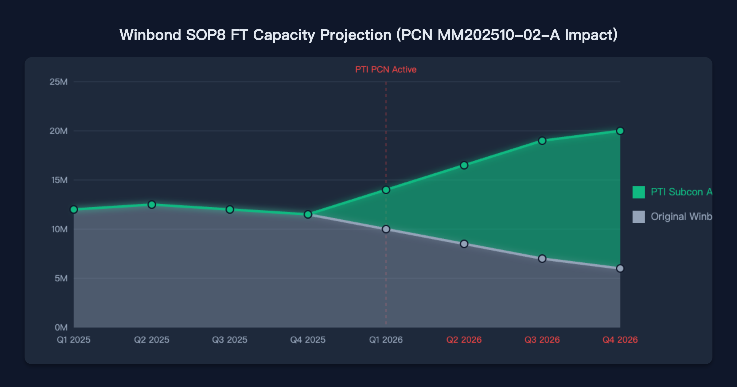
This strategic PCN confirms that Winbond intends to support the SOP8 form factor for years to come. During the initial Q1 2026 factory transition, spot market allocations briefly tightened. However, using advance PCN intelligence, the icallin procurement team secured massive bulk reserves of the W25Q128JVSIQ (Industrial Temperature, -40°C to +85°C) to bridge the gap.
2. The Engineer's Nightmare: W25Q128JVSIQ Boot-Loops
Securing the stock is excellent news. But deploying it requires navigating a brutal hardware trap. If your firmware engineering team works with legacy embedded Linux kernels, Xilinx Vivado, or older U-Boot builds, the W25Q128JVSIQ has been known to mysteriously "brick" custom IoT gateways on first power-up.
The "Q" Suffix Trap: Hard-Coded Quad Enable (QE) Registers
The root cause of the infamous Winbond boot-loop lies in the exact part number nomenclature. The letter "Q" at the end of W25Q128JVSIQ isn't just a random batch code; it explicitly designates that the Quad Enable (QE) bit is permanently set to 1 in the Status Register-2 (SR-2) leaving the factory.
W25Q128JVSIM (M suffix) = QE bit is 0 (Standard SPI).
W25Q128JVSIQ (Q suffix) = QE bit is 1 (Quad I/O active).
The Architectural Disaster:
In Standard SPI or Dual SPI applications, the flash chip has /WP (Write Protect) on Pin 3 and /HOLD (Hold) on Pin 7. If a hardware designer ties these pins to $V_{CC}$ (a standard practice to safely ignore them), the chip works perfectly.
However, when the QE bit is forced to 1 (which it is on the "Q" variant), Pin 3 and Pin 7 physically change their internal routing functionality. They cease to be /WP and /HOLD pins and instantly transform into I/O2 and I/O3 for Quad-SPI data lines.
If your U-Boot instance, unaware of this hard-coded factory state, attempts to send a specific Write Status Register command (01h) or expects standard /WP functionality, the flash memory enters a locked state. The SPI bus returns trailing 0xFF garbage bytes, MD5 checksums fail, and your IoT gateway spins in an infinite boot loop.
Table 1: W25Q128JV Status Register Conflict Matrix
| Pin Function / Firmware Attempt | W25Q128JVSIM (QE=0) Expected Behavior | W25Q128JVSIQ (QE=1) Catastrophic Reality |
|---|---|---|
| Pin 3 physically tied to GND | Hardware Write Protection is ON | Fatal Data Short. Pin 3 tries to output data into GND. |
U-Boot sf probe generic call | Returns 3-byte JEDEC ID perfectly | Sometimes misidentifies due to unexpected Quad state |
| Attempting to clear SR-2 via code | Works as intended | Fails or is ignored (QE is OTP / Non-volatile on Q versions) |
U-Boot & Legacy SPI Conflict Resolution Strategies
If your supply chain has purchased 50,000 reels of the W25Q128JVSIQ because of the PCN safety but your boards only support standard Dual-SPI routing, you must fix this in your device tree (.dts) or bootloader config immediately:
- Kernel Configuration: In newer Linux kernels, ensure the
CONFIG_SPI_FLASH_WINBONDflag is active, and specifically ensure your Device Tree specifiesspi-tx-bus-width = <1>;or<2>;to force the kernel driver to ignore the QSPI lines completely during standard reads. - U-Boot Flags: Check if your U-Boot version includes specific
SPI_NOR_HAS_LOCKflags. You may need to patchspi_flash_probe()to stop it from trying to read standard SR protection bits that are masked by the Q-series architecture. - Hardware Redesign Warning: If you are laying out a new PCB for the "Q" chip but only plan to use Standard SPI, DO NOT directly ground Pin 3 or Pin 7 thinking they are just
/WPpins. You must leave them floating or pull them up softly with a strong 10kΩ resistor to prevent dead-shorting an active Data I/O line during a read cycle.
Top 5 Cross-Reference SPI Nor Flash Alternatives
If modifying your U-Boot kernel is impossible and you absolutely must seek a drop-in replacement that defaults to standard SPI (QE=0), or if you simply need alternative sources for the SOP8 208-mil 128Mb package, here are the top 5 verified cross-references available on the global market:
- Macronix MX25L12835FM2I-10G — 🟢 Direct Drop-In: A legendary Taiwanese memory alternative. Perfect pin-to-pin and JEDEC command-set compatibility (104MHz native).
- GigaDevice GD25Q128ESIG — 🟢 High-Volume Mainstay: Dominates the domestic Asian router market. Identical 133MHz Quad-SPI architecture in the exact same 208-mil body. Code-compatible with Winbond reads.
- Infineon S25FL128SAGMFI011 — 🟡 Premium Automotive-Grade: Originally Cypress Semiconductor IP. Requires minor bootloader code modifications to read the unique Cypress JEDEC manufacturer ID (
01h), but incredibly reliable. - Micron MT25QL128ABA8ESF-0SIT — 🟡 Industrial Grade Architecture: Highly robust flash array structure. It comes with a premium price tag aimed at aerospace/telecom routers rather than consumer electronics.
- ISSI IS25LP128F-JBLE — 🟢 The Protocol Matcher: Supports seamless 133MHz fast reads while maintaining flawless backward compatibility to the Winbond instruction-set architecture and SOP8 footprint.
3. onsemi NTMFS5C430NLT1G: Driving AI Server Power Density
While legacy flash memory fights for testing capacity and fights firmware bugs, a completely different war is raging in discrete power semiconductors. The explosive expansion of Nvidia Grace Blackwell (GB200) architectures and 1U ultra-dense AI server nodes has pushed intermediate bus Voltage Regulator Modules (VRMs) to their absolute physical limits.
The onsemi NTMFS5C430NLT1G—a 30V single N-Channel MOSFET—has emerged as the universally desired workhorse for secondary-side synchronous rectification.
1.4 mΩ Resistance: The Thermal Mathematics of 200 Amps
In telecom infrastructure and data center racks, DC-DC converter efficiency is measured in fractions of a percent. When a multiphase VRM steps a 12V bus down to a 0.8V core rail capable of supplying massive H100 GPU arrays, the secondary-side low-side MOSFETs frequently conduct over 150 Amps of continuous phase current.
At these extreme currents, Ohm's law ($P = I^2R$) rules data center existence. Conduction loss dictates survival. The onsemi NTMFS5C430NLT1G possesses an absolute maximum drain current ($I_D$) of 200A and a staggering typical ON-Resistance ($R_{DS(on)}$) of just 1.4 mΩ when driven with a standard 10V gate signal.
Let's execute the raw thermal mathematics if a server node demands 150 Amps of continuous current:
Generic 30V MOSFET (5.0 mΩ): $$ P_{DISSIPATION} = (150A)^2 \times 0.005\Omega = \mathbf{112.5 Watts} $$ (Result: The 5x6mm package immediately enters thermal runaway, melts the FR-4 PCB fiberglass, and triggers a server rack fire alarm.)
Using the 1.4 mΩ onsemi NTMFS5C430NLT1G: $$ P_{DISSIPATION} = (150A)^2 \times 0.0014\Omega = \mathbf{31.5 Watts} $$ (Result: A brutal but manageable thermal load easily extracted by high-velocity 15,000 RPM server fans and pure copper heat pipes).
DFN5 (SO-8FL) Package Mechanics & Clip Bonding
What makes the NTMFS5C430NLT1G genuinely revolutionary is that it packs this 200A capability into a microscopic DFN5 (5x6 mm) footprint, commonly referred to as SO-8FL. Historically, achieving sub-2mΩ resistance required monstrous D2PAK or TO-220 packages.
By utilizing advanced copper clip-bonding techniques internally rather than standard frail aluminum wire bonds, onsemi virtually eliminated package inductance. This dramatically lowers the Gate Charge ($Q_{G}$ is only 46 nC typical). A lower $Q_G$ means the gate driver IC doesn't waste energy filling parasitic "buckets," allowing the VRM buck converter to switch at 1MHz+ frequencies without suffering catastrophic switching losses.
4. The 200A AI Server VRM Trap: Underdamped Ringing & $dv/dt$ Catastrophe
Securing the onsemi MOSFET is a massive win for your purchasing department. But just like the Winbond Flash, throwing this ultimate component onto a PCB without understanding the physics will lead to immediate explosions.
Parasitic Inductance Meets Lightning-Fast Switching
If you replace an older, slower MOSFET with the ultra-fast NTMFS5C430NLT1G and power your test bench, you may suddenly find the MOSFET detonating despite running well below its 30V/200A limits. Why? Severe Switch-Node Ringing.
Ringing is fundamentally an underdamped RLC resonance triggered by high-speed switching transitions ($dv/dt$ and $di/dt$).
- The Exciter: The onsemi chip is so fast, its turn-on/turn-off edges are almost vertical.
- The Parasitic Tank: Your PCB traces, the vias acting as return paths, and the intrinsic capacitance of the MOSFET ($C_{oss}$) form a microscopic inductor-capacitor (LC) oscillator.
When the MOSFET snaps shut at 100 Amps, the massive $di/dt$ slams into the tiny parasitic inductance ($L_{parasitic}$) of your PCB layout. According to $V = L (di/dt)$, this generates an enormous back-EMF voltage spike on the Drain pin. Instead of seeing a safe 12V bus voltage, the Switch-Node instantly rings up to 45V+, instantly exceeding the absolute maximum $V_{DSS}$ rating (30V) and violently puncturing the silicon oxide gate.
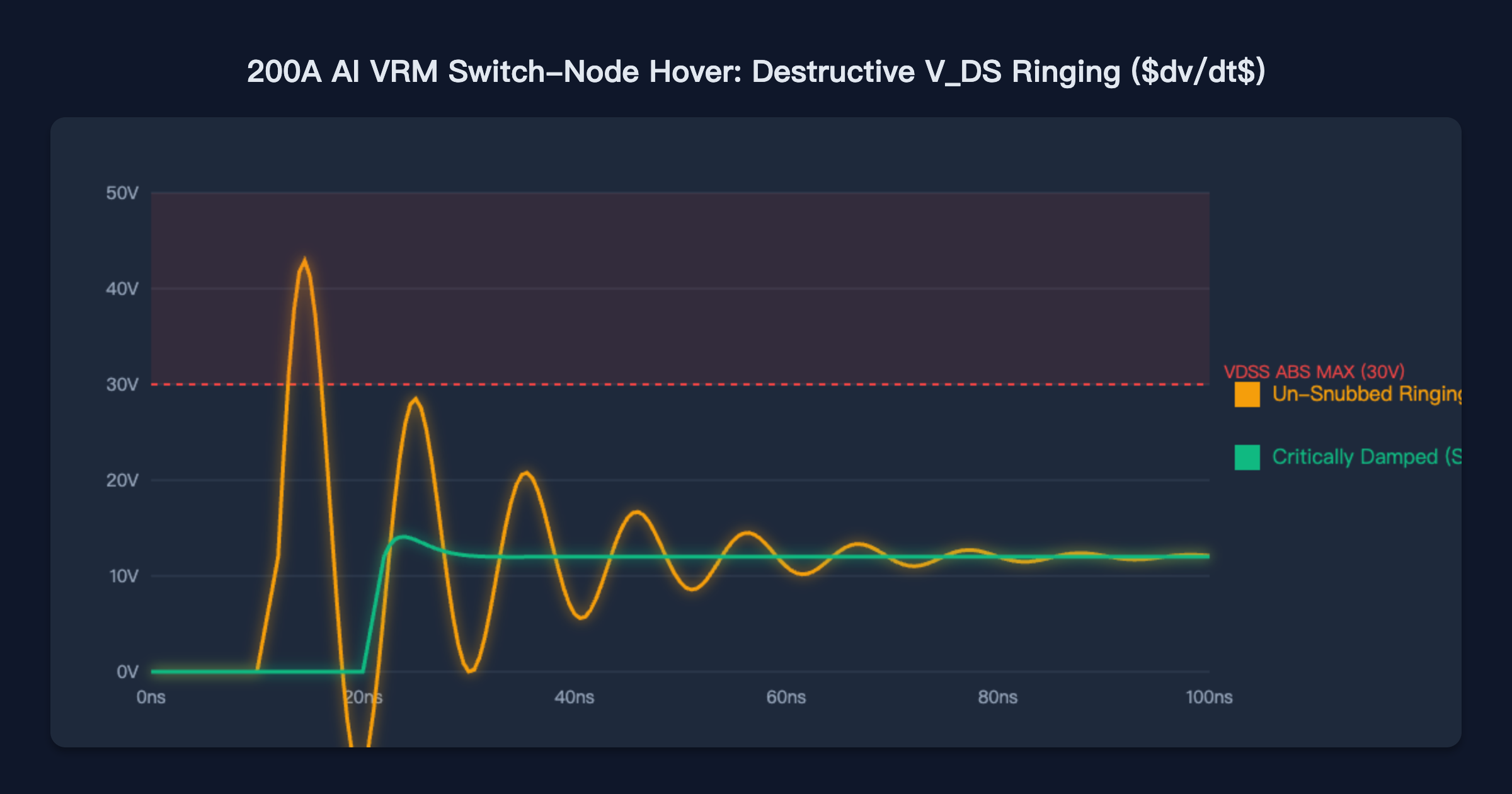
RC Snubber Design: Dampening the Ringing Waveform
To safely deploy this 200A silicon beast, you must actively dampen the resonance. Beyond minimizing the physical PCB layout loop area (bringing your input ceramic capacitors within millimeters of the Drain pin), power engineers must calculate and install an RC Snubber circuit.
An RC Snubber is a small resistor and capacitor placed in series directly across the MOSFET's Drain and Source. It acts as an energy absorber that critically dampens the high-frequency oscillation.
The Math (How to Calculate the Snubber for the NTMFS5C430NLT1G):
- Locate $C_{\text{parasitic}}$: Look at the onsemi datasheet. The Output Capacitance ($C_{oss}$) at 15V is roughly $1700\text{ pF}$.
- Measure Ringing Frequency ($f_{ring}$): Use a high-bandwidth 1GHz oscilloscope (using a tip-and-barrel, zero-ground-wire probe) to measure the destructive ringing wave. Let's assume it rings at $150\text{ MHz}$.
- Calculate Parasitic Inductance ($L_P$): $$ L_P = \frac{1}{(2\pi \times f_{ring})^2 \times C_{oss}} \approx \mathbf{0.66\text{ nH}} $$ (This tiny $0.66\text{ nH}$ is what destroys your board!)
- Calculate Snubber Resistor ($R_{snubber}$): It must equal the characteristic impedance of the tank: $$ R_{snubber} = \sqrt{\frac{L_P}{C_{oss}}} = \sqrt{\frac{0.66 \times 10^{-9}}{1700 \times 10^{-12}}} \approx \mathbf{0.6 \text{ }\Omega} $$
- Calculate Snubber Capacitor ($C_{snubber}$): Rule of thumb is 3 to 4 times $C_{oss}$. So roughly $\mathbf{6800\text{ pF}}$.
By adding a highly rated, low-inductance $0.6 \Omega$ resistor and a $6.8\text{ nF}$ ceramic capacitor directly across the DFN5 pads, you will completely flatten the ringing curve, allowing the NTMFS5C430NLT1G to safely push its terrifying 200A load.
Top 5 30V/200A AI Server MOSFET Alternatives
Because the NTMFS5C430NLT1G is aggressively allocated to Tier-1 Server ODMs (Wistron, Foxconn, Quanta), spot market inventory can tighten rapidly. If you must migrate your VRM sync-rectifier design to another vendor, these are the top 5 leading 5x6mm equivalents that match the thermal mathematics:
- Infineon BSC014N03LS G — 🟢 OptiMOS™ Match: The legendary German counterpart. 30V, 1.4mΩ, housed in the identical SuperSO8 footprint. World-class thermal dissipation.
- Texas Instruments CSD17578Q5A — 🟡 NexFET™ Architecture: 30V, 1.6mΩ. Slightly higher on-resistance but offers incredibly low gate impedance for ultra-high-frequency (1.5MHz+) switching capability.
- Toshiba TPH1R204PL — 🟢 Japanese Reliability Benchmark: 40V, 1.2mΩ. Provides an extra 10V of voltage headroom (excellent for absorbing VRM ringing) while keeping resistance microscopic.
- AOS AON6512 — 🟡 The Aggressive Disruptor: 30V, 1.4mΩ. Often leveraged by cost-conscious motherboard manufacturers targeting aggressive pricing tiers without sacrificing the 200A capability.
- Vishay SiRA52DP — 🟢 TrenchFET® Gen IV: 40V, 1.3mΩ. Extremely rugged gate oxide structure engineered specifically to survive voltage transient spikes in telecom base stations.
5. The Counterfeit Market: Why Origin Traceability Matters
If a counterfeit MCU fails, a router refuses to boot. If a counterfeit 200A VRM MOSFET fails, standard FR-4 fiberglass PCBs will literally ignite, destroying a $50,000 AI hardware accelerator in a split second.
Blacktop Fakes on High-Current DFN5 MOSFETs
Because discrete MOSFETs like the NTMFS5C430NLT1G are "dumb" analog power components with no encrypted digital signatures to query via JTAG, they are the number one target for gray market operations. Unscrupulous brokers will acquire reels of cheap, consumer-grade 30V/30A DFN5 MOSFETs possessing a horrific 15mΩ resistance. They sand off the original plastic markings (blacktopping) and laser-engrave the valuable 5C430L designator onto the casing.
In an idle state, the fake chip tests perfectly fine on a multimeter. However, the moment an AI server attempts to pull 150 Amps through the fake chip's thin internal die, it generates over 300 Watts of heat and instantly combusts.
AS6081 Zero-Trust Testing Protocols for Memory & Silicon
At icallin's In-House Verification Lab, we approach high-power discrete silicon with a strict Zero-Trust AS6081 testing methodology.
- Chemical Decapsulation: We utilize boiling fuming nitric acid to dissolve the epoxy resin, physically exposing the silicon die to verify the complex Trench gate structure and massive copper-clip metallization specifically engineered by onsemi.
- Real-Time X-Ray Imaging: For the W25Q128JVSIQ Flash, we scan the SOP8 packages to confirm exact wire-bond geometries, ensuring we are not receiving downgraded 64Mbit or 32Mbit silicon dies re-balled inside an empty SOP8 shell.
- High-Power Curve Tracing: We run parametric $I_D$ vs $V_{DS}$ boundary tests to ensure the MOSFET can truly conduct 200A without the $R_{DS(on)}$ degrading beyond 1.4mΩ parameters.
6. icallin Supply Chain Intelligence & Procurement Guarantee
For procurement directors managing NPI prototypes or volume data center production, waiting 40 weeks for Winbond memory or onsemi power discretes is no longer an acceptable business strategy. Engineering teams cannot wait a year for a single reel of flash to test a U-Boot firmware patch.
Because of our active monitoring of Winbond PCN capacity distributions and our aggressive forward-stocking of critical sync-rectifier MOSFETs entering the AI hardware boom, icallin.com is currently holding substantial, fully traceable warehouse inventory of both the W25Q128JVSIQ and the NTMFS5C430NLT1G.
7. Frequently Asked Questions (FAQ)
Q1: How do I fix the W25Q128JVSIQ boot-loop in my older U-Boot or Linux kernel environments?
You must prevent the bootloader from writing to the Status Register 2 (SR-2). The "Q" suffix variant has its Quad Enable (QE) bit permanently locked to 1. If your custom IoT gateway does not support Quad-SPI hardware routing, you must configure your device tree to spi-tx-bus-width = <1>; or utilize software patches to ignore the Quad I/O capability altogether.
Q2: Does the PTI Final Test site addition (PCN MM202510-02-A) change the physical or electrical characteristics of the Flash memory?
No. Winbond explicitly classified this as a testing capacity expansion only. The silicon die fabrication, circuit layout, and physical SOP8 lead framing remain completely identical. Your engineering team does not need to re-qualify the part electrically, but you must ensure your procurement software is updated to recognize chips emerging from the PTI site.
Q3: Why does my VRM circuit using the NTMFS5C430NLT1G experience severe switch-node voltage overshoot (ringing)?
Because the MOSFET turns on and off incredibly fast ($dv/dt$). The highly aggressive switching speed excites microscopic parasitic trace inductances ($L_{parasitic}$) present on your PCB layout and the parasitic output capacitance ($C_{oss}$) of the silicon itself. This creates an LC oscillation loop that generates enormous back-EMF voltage spikes.
Q4: What is the formula for calculating an RC snubber value for standard DFN5 (SO-8FL) packages running at 1MHz+?
The resistance ($R_{snubber}$) should match the characteristic impedance of your parasitic tank circuit: $R_{snubber} = \sqrt{\frac{L_P}{C_{oss}}}$. The capacitance ($C_{snubber}$) is generally chosen to be 3x to 4x the value of the intrinsic $C_{oss}$. Keep in mind that snubbers pull energy out of the resonant tank and dissipate it as heat, so use a power-rated resistor.
Q5: How do I verify a genuine onsemi NTMFS5C MOSFET vs. a relabeled gray market fake?
Visual inspection of the laser etchings is completely insufficient for high-demand AI components. You must engage a distributor that utilizes rigorous AS6081 testing standards. This mandates chemical decapsulation (acid etching to expose the die), X-ray inspection to analyze the clip-bonds, and high-power dynamic curve tracing to verify the 1.4 mΩ paramater limits.
Q6: Can I get a partial reel of these components, or must I order full factory reels?
Depending on current warehouse allocations and static tape breakdown limits, icallin frequently supports high-mix prototyping (NPI) runs with precision cut-tape quantities or partial reels. Please contact our sales engineering floor with your exact target timeline and quantity requirements.
*Charles·Lee is a Senior Semiconductor Supply Chain Analyst at icallin.com, specializing in cross-reference engineering, ESD protection architectures, and FPGA procurement strategy. With over a decade of experience bridging the gap between hardware design teams and global component distribution networks, Charles helps enterprise customers navigate allocation crises, validate drop-in replacements, and secure authentic inventory through AS6081-certified channels.

Top Recommended part