XCKU5P-2FFVB676I In Stock: Kintex UltraScale+ FPGA for 5G & Edge AI
Xilinx UltraScale+ FPGA Hot Stock: XCKU5P-2FFVB676I — Verified Inventory for 5G & Edge Computing
Category: Market Trends & Lead Times | Author: Charles·Lee | Published: May 2026 | Last Updated: May 8, 2026
Key Takeaways:
- The XCKU5P-2FFVB676I is a 16nm FinFET+ Kintex UltraScale+ FPGA delivering 474,600 logic cells, 1,824 DSP48E2 slices, and 16 GTY transceivers at 32.75 Gb/s — the workhorse for 5G O-RAN, edge AI inference, and radar signal processing.
- Factory lead times have stretched to 22 weeks as AMD reallocates TSMC 16nm capacity toward Versal AI Edge and data center accelerators, while unit pricing ranges from $2,700 to $5,200 depending on volume and source.
- The FFVB676 package (27×27mm) is footprint-compatible with the lower-cost XCKU3P-2FFVB676I, enabling pin-compatible downgrade without PCB redesign.
- PCN XCN24003 confirms AMD rebranding does not affect form, fit, or function — but counterfeit risk in broker channels remains elevated, with Xilinx FPGAs ranking in ERAI's top 5 most counterfeited semiconductor families.
- icallin.com maintains factory-sealed, traceable XCKU5P-2FFVB676I inventory for immediate shipment, bypassing the 22-week factory queue. Submit an RFQ →
Executive Summary — Why XCKU5P-2FFVB676I Is the FPGA Procurement Challenge of the Moment
The semiconductor industry's AI-driven supercycle has created an unexpected casualty: mid-range FPGAs. While headlines focus on GPU shortages and HBM allocation wars, the Kintex UltraScale+ family — AMD's (formerly Xilinx's) price-performance sweet spot for 5G infrastructure, defense electronics, and industrial computing — is quietly becoming one of the hardest components to procure in 2026.
The XCKU5P-2FFVB676I sits at the epicenter of this squeeze. With 474,600 system logic cells, 1,824 DSP slices optimized for wideband signal processing, and 16 GTY transceivers capable of 32.75 Gb/s line rates, this device powers the digital front-end of 5G mMIMO radio units, the channelization engines of electronic warfare receivers, and the inference pipelines of edge AI accelerators. It is, by any measure, a mission-critical component — and its supply is tightening.
Factory lead times from AMD's authorized distribution network have stretched to approximately 22 weeks. Unit pricing in the open market has escalated to the $2,700–$5,200 range, reflecting a combination of genuine scarcity and speculative broker markups. And the counterfeit risk is real: ERAI's annual report consistently places Xilinx-branded FPGAs among the top 5 most counterfeited semiconductor device families, with remarked speed grades and recycled telecom pulls representing the most common fraud vectors.
This technical procurement brief serves three purposes: first, to provide a datasheet-sourced deep specification review so that engineering teams understand exactly what they are specifying; second, to contextualize the supply chain dynamics driving the current shortage; and third, to present icallin.com's verified inventory position and a 5-model procurement matrix that gives procurement managers actionable alternatives.
| Parameter | XCKU5P-2FFVB676I Snapshot |
|---|---|
| Architecture | Kintex UltraScale+ (16nm FinFET+) |
| System Logic Cells | 474,600 |
| DSP48E2 Slices | 1,824 |
| Block RAM | 16.9 Mb (480 blocks) |
| UltraRAM | 18.0 Mb (64 blocks) |
| GTY Transceivers | 16 × 32.75 Gb/s |
| User I/O | 72 HD + 208 HP = 280 |
| Package | FFVB676 (27×27mm, 1.0mm pitch) |
| Speed / Temp Grade | -2 / Industrial (-40°C to +100°C) |
| Factory Lead Time | ~22 weeks |
| Market Price Range | $2,700 – $5,200 (qty-dependent) |
| Counterfeit Risk | HIGH (ERAI top-5 family) |
Table 1: XCKU5P-2FFVB676I Procurement Snapshot | Source: AMD DS890 v4.8, Market Intelligence Q2 2026 | Compiled by: icallin.com
XCKU5P-2FFVB676I Deep Specification Review — What Makes This FPGA Mission-Critical
Understanding the XCKU5P's architectural advantages is essential for both design engineers validating their component selection and procurement managers assessing substitution risk. The specifications below are sourced directly from AMD's DS890 UltraScale Architecture and Product Data Sheet (v4.8, November 2025).
16nm FinFET+ Architecture
The Kintex UltraScale+ family is fabricated on TSMC's 16nm FinFET+ process node — the same node used for AMD's Versal AI Edge and Zynq UltraScale+ MPSoC families. This process delivers a compelling combination of performance per watt and transistor density that positions the KU5P between the cost-optimized Artix UltraScale+ and the resource-rich Virtex UltraScale+ families.
The UltraScale+ architecture introduces several key improvements over the previous UltraScale (20nm) generation: UltraRAM blocks for high-density on-chip storage, enhanced DSP48E2 slices with wider pre-adders and XOR logic, and GTY transceivers with higher line rates.
Logic and DSP Resources
The XCKU5P provides 474,600 system logic cells organized into Configurable Logic Blocks (CLBs), each containing 6-input look-up tables (LUTs) and flip-flops. In raw terms, this translates to 216,960 CLB LUTs and 433,920 CLB flip-flops — sufficient for implementing complex 5G digital front-end chains including CFR (Crest Factor Reduction), DPD (Digital Pre-Distortion), and multi-carrier channelization filters simultaneously.
The 1,824 DSP48E2 slices represent the KU5P's signal processing backbone. Each slice contains a 27×18 twos-complement multiplier, a 48-bit accumulator, a pre-adder for symmetric filter optimization, and a 96-bit-wide XOR unit for FEC and CRC acceleration. At maximum clock rates, the KU5P's DSP array delivers over 1.4 TMAC/s (trillion multiply-accumulate operations per second) — competitive with dedicated ASIC signal processors at a fraction of the NRE cost.
Memory Hierarchy
The KU5P's on-chip memory architecture combines two complementary technologies:
| Memory Type | Block Count | Total Capacity | Width | Depth | Features |
|---|---|---|---|---|---|
| Block RAM (BRAM) | 480 | 16.9 Mb | 36-bit (72-bit in SDP) | 512–16K | Built-in FIFO, ECC |
| UltraRAM | 64 | 18.0 Mb | 72-bit | 4K | Cascade-capable, 1-cycle latency |
| Distributed RAM | — | 6.1 Mb max | Configurable | LUT-based | Fastest access, lowest latency |
| Total On-Chip | — | ~41 Mb | — | — | — |
Table 2: XCKU5P On-Chip Memory Hierarchy | Source: AMD DS890 v4.8 | Compiled by: icallin.com
The 18.0 Mb of UltraRAM is a differentiating feature exclusive to UltraScale+ devices. Each UltraRAM block provides a 4Kx72 single-port or simple dual-port memory with single-cycle access latency and cascade capability — enabling the construction of large, contiguous memory arrays without consuming BRAM resources. For edge AI applications, UltraRAM serves as on-chip weight storage for neural network models, eliminating the latency and power penalty of external DDR access during inference.
High-Speed Serial Transceivers
The XCKU5P-2FFVB676I integrates 16 GTY transceivers, each capable of line rates up to 32.75 Gb/s. These transceivers support a comprehensive protocol stack including 25G Ethernet, PCIe Gen3 x8, CPRI/eCPRI, JESD204B/C, and custom serial protocols.
In the FFVB676 package specifically, the 16 GTY transceivers are organized into 4 quads, each served by a fractional PLL (8 fractional PLLs total). This arrangement enables simultaneous operation at multiple line rates — for example, 4 lanes of 25G Ethernet for fronthaul connectivity and 8 lanes of 10G CPRI for legacy radio unit interfaces, all within a single device.
I/O and Package Details
The FFVB676 package provides 280 user I/O pins organized into two categories:
- 72 HD (High-Density) I/Os: Supporting voltages from 1.2V to 3.3V, suitable for low-speed control interfaces, GPIO, and legacy parallel buses
- 208 HP (High-Performance) I/Os: Supporting voltages from 1.0V to 1.8V, designed for high-speed memory interfaces (DDR4 up to 2,400 Mb/s) and LVDS signaling
The package measures 27×27mm with 1.0mm ball pitch — a compact form factor that enables deployment in size-constrained platforms such as small-cell radio units, mezzanine cards, and ruggedized defense subsystems.
Market Intelligence — Why XCKU5P Supply Is Tightening
The XCKU5P supply shortage is not an isolated event but rather a symptom of three converging macro-level dynamics in the semiconductor industry.
Dynamic 1: TSMC 16nm Wafer Allocation Wars
AMD's FPGA product portfolio shares TSMC's 16nm FinFET+ production capacity with its Versal AI Edge, Zynq UltraScale+ MPSoC, and legacy UltraScale product lines. As demand for Versal AI Edge devices surges — driven by hyperscaler deployments of AI inference accelerators — AMD has been strategically reallocating wafer starts away from mature UltraScale+ products toward higher-margin Versal silicon.
The result is a classic capacity cannibalization scenario: the XCKU5P's wafer allocation is being squeezed not by declining demand for the XCKU5P itself, but by exploding demand for a sibling product family competing for the same fab capacity.
Dynamic 2: 5G mMIMO Deployment Acceleration
The global rollout of 5G massive MIMO (mMIMO) antenna systems has entered its acceleration phase. Each O-RAN-compliant radio unit typically consumes 1–2 Kintex UltraScale+ FPGAs for digital front-end processing — including channelization, CFR/DPD, and eCPRI/CPRI protocol bridging. With tier-1 operators deploying tens of thousands of radio units per quarter across Asia-Pacific, North America, and Europe, the aggregate demand for XCKU5P-class devices has outpaced AMD's ability to fulfill orders within standard lead times.
Dynamic 3: Defense and Aerospace Priority Allocation
ITAR-controlled defense programs receive priority allocation from AMD's government and aerospace division. These programs consume significant volumes of industrial-grade (-I suffix) Kintex UltraScale+ devices for radar processing, electronic warfare, signals intelligence, and secure communications. The defense allocation effectively creates a "hidden demand" layer that reduces the available supply pool for commercial and industrial customers.
PCN Impacts
Two recent Product Change Notices are relevant to XCKU5P procurement:
PCN XCN24003 (May 2024): AMD is transitioning all Xilinx 7-series and newer products from Xilinx branding to AMD branding. This affects package markings and associated packaging materials. Critically, there are no changes to form, fit, function, or reliability. However, the rebranding has created procurement chain confusion, with some quality systems flagging AMD-marked devices as "non-conforming" against BOMs that specify Xilinx part numbers.
PCN XCN20014 (v1.4, May 2021): AMD added Nanya Technology as a secondary substrate supplier for UltraScale and UltraScale+ monolithic packages, including XCKU5P in FFVB676. This change improves supply chain resilience by reducing dependence on a single substrate source, but devices with Nanya substrates may require re-qualification in some high-reliability programs.
| Risk Factor | Severity | Trend | Mitigation |
|---|---|---|---|
| TSMC 16nm wafer allocation squeeze | 🔴 High | Worsening | Secure verified spot inventory immediately |
| 5G mMIMO demand surge | 🔴 High | Stable-High | Lock multi-quarter allocations with distributors |
| Defense priority allocation | 🟡 Medium | Stable | Source from independent distributors with commercial allocation |
| AMD rebranding confusion (XCN24003) | 🟢 Low | Declining | Update QMS to accept both Xilinx and AMD markings |
| Nanya substrate qualification (XCN20014) | 🟢 Low | Resolved | Verify substrate COC matches your approved vendor list |
| Counterfeit risk in broker market | 🔴 High | Worsening | Purchase only from verified sources with full traceability |
Table 3: XCKU5P-2FFVB676I Supply Chain Risk Matrix | Source: icallin.com Market Intelligence | Compiled by: icallin.com

Application Deep Dive — Where XCKU5P-2FFVB676I Delivers Maximum Value
The XCKU5P's resource profile — balanced logic density, heavy DSP, wide transceiver bandwidth, and generous on-chip memory — makes it uniquely suited for applications that require real-time, high-throughput signal processing in thermally and physically constrained environments.
5G O-RAN Radio Units
The Open RAN architecture has transformed the 5G radio access network from a monolithic, vendor-locked ecosystem into a disaggregated, multi-vendor platform. At the heart of every O-RAN-compliant radio unit sits an FPGA performing the computationally intensive digital front-end (DFE) functions:
- Channelization: Multi-carrier filtering and frequency translation across 100 MHz or 200 MHz instantaneous bandwidths, consuming hundreds of DSP slices for polyphase filter banks
- CFR/DPD: Crest Factor Reduction and Digital Pre-Distortion linearize the power amplifier, requiring tight feedback loops with sub-microsecond latency — achievable only in FPGA fabric, not in software-defined implementations
- eCPRI/CPRI Bridging: The 16 GTY transceivers at 32.75 Gb/s enable simultaneous fronthaul connectivity (25G eCPRI to the DU) and legacy radio interface support (10G CPRI to older baseband units)
The XCKU5P's 1,824 DSP slices and 34.9 Mb on-chip memory provide sufficient resources to implement a complete 4T4R mMIMO DFE chain — including beamforming weight application — within a single device.
Edge AI Inference Accelerators
The convergence of FPGA-based inference and the UltraRAM memory hierarchy creates a compelling edge AI platform. The XCKU5P's 18.0 Mb of UltraRAM can store the weight matrices of quantized (INT8/INT4) neural network models entirely on-chip, eliminating the latency and power penalty of external DDR4 access during inference.
For CNN-based image classification and object detection workloads, the 1,824 DSP48E2 slices — each capable of one INT8 multiply-accumulate per clock cycle — deliver over 3.6 TOPS (INT8) at 500 MHz clock speeds. This performance level handles real-time inference on multiple video streams simultaneously, making the XCKU5P suitable for multi-camera industrial inspection systems and autonomous mobile robot perception pipelines.
Radar and Electronic Warfare
Defense applications exploit the XCKU5P's combination of wide transceiver bandwidth and deep DSP resources for wideband channelization, pulse compression, and adaptive beamforming. The industrial temperature grade (-40°C to +100°C) meets MIL-STD-810 environmental requirements without requiring expensive ruggedized packaging, while the FFVB676's compact 27×27mm footprint fits within the tight space constraints of phased array antenna modules.
Industrial Machine Vision
Multi-camera image acquisition systems use the XCKU5P's HP I/O banks for MIPI CSI-2 or SLVS-EC camera interfaces, while the FPGA fabric implements real-time image preprocessing (debayering, HDR merge, defect detection) at line rates exceeding 1 Gpixel/s. The combination of high-speed I/O and parallel processing capability eliminates the frame-rate bottlenecks inherent in CPU/GPU-based vision pipelines.
| Application | LUT Usage | DSP Usage | Memory Usage | Transceiver Usage | Key Advantage |
|---|---|---|---|---|---|
| 5G O-RAN 4T4R DFE | ~65% | ~80% | ~70% BRAM, ~50% URAM | 8–12 GTY (25G eCPRI) | Real-time DPD with sub-µs latency |
| Edge AI (INT8 CNN) | ~50% | ~90% | ~30% BRAM, ~85% URAM | 1–4 GTY (PCIe Gen3) | 3.6+ TOPS on-chip inference |
| Wideband Radar Channelizer | ~55% | ~75% | ~60% BRAM, ~40% URAM | 4–8 GTY (ADC/DAC IF) | 1 GHz IBW channelization |
| Multi-Camera Vision (4×) | ~45% | ~40% | ~50% BRAM, ~20% URAM | 0 (parallel I/O) | >1 Gpixel/s pipeline |
Table 4: Application-Specific XCKU5P Resource Utilization Estimates | Source: icallin.com Engineering Analysis | Compiled by: icallin.com
Kintex UltraScale+ Family Migration & Package Compatibility Guide
One of the most powerful features of AMD's UltraScale+ architecture is footprint compatibility across device densities. Understanding these migration paths is essential for procurement teams seeking alternative sourcing options when the primary target device is unavailable.
FFVB676 Footprint Compatibility
The FFVB676 package (27×27mm, 1.0mm ball pitch, 676 balls) is shared by two Kintex UltraScale+ devices:
- XCKU5P-2FFVB676I: 474K logic cells, 1,824 DSP, 16 GTY, 72 HD + 208 HP I/O
- XCKU3P-2FFVB676I: 355K logic cells, 1,368 DSP, 16 GTY, 72 HD + 208 HP I/O
These two devices share an identical ball map in the FFVB676 package. A PCB designed for the XCKU5P can accept the XCKU3P without any layout modification — the only difference is the available logic, DSP, and memory resources. For designs that do not fully utilize the KU5P's capacity, the KU3P represents a lower-cost, immediately available alternative that drops directly into the same footprint.
Speed Grade Options Within FFVB676
The XCKU5P is available in three speed grades within the FFVB676 package, each offering a different performance-cost tradeoff:
- -1 (Commercial/Industrial): XCKU5P-1FFVB676I — lowest cost, suitable for designs with comfortable timing margins
- -2 (Industrial): XCKU5P-2FFVB676I — the primary target of this analysis, offering the optimal balance of performance and industrial temperature range
- -3 (Extended Performance): Highest clock frequencies, typically reserved for designs requiring maximum throughput at the expense of higher power consumption
Upward Migration Paths
For designs requiring more logic resources, DSP capacity, or transceiver count than the XCKU5P provides, two upward migration options exist within the Kintex UltraScale+ family:
- XCKU9P-2FFVE900I (FFVE900, 31×31mm): 599K logic cells (+26%), 2,520 DSP (+38%), 28 GTH transceivers at 16.3 Gb/s. Note the transceiver type change from GTY to GTH, which reduces maximum line rate but may be acceptable for applications not requiring 25G+ connectivity.
- XCKU11P-1FFVA1156E (FFVA1156, 35×35mm): 653K logic cells (+38%), 2,928 DSP (+60%), 32 GTH transceivers + 8 GTY transceivers, 416 HP I/O. This device doubles the transceiver count and significantly expands logic resources, but requires a PCB redesign to accommodate the larger package.
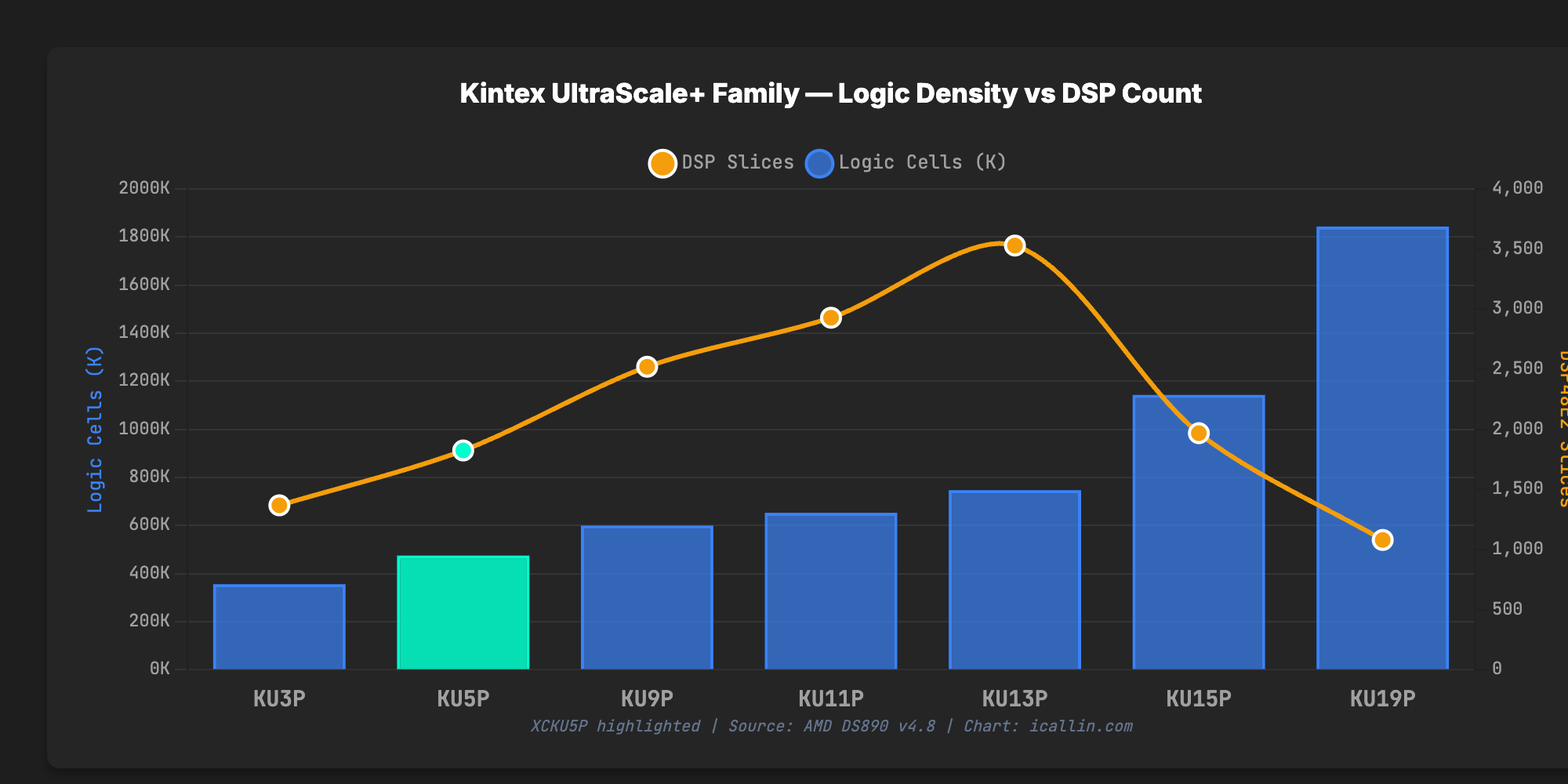
| Model | Logic Cells | DSP | BRAM (Mb) | URAM (Mb) | Transceivers | Package | Footprint Compatible? |
|---|---|---|---|---|---|---|---|
| XCKU3P | 355,950 | 1,368 | 12.7 | 13.5 | 16 GTY | FFVB676 (27×27) | ✅ Yes — same ball map |
| XCKU5P | 474,600 | 1,824 | 16.9 | 18.0 | 16 GTY | FFVB676 (27×27) | ✅ Primary target |
| XCKU9P | 599,550 | 2,520 | 32.1 | 0 | 28 GTH | FFVE900 (31×31) | ❌ Larger package |
| XCKU11P | 653,100 | 2,928 | 21.1 | 22.5 | 32 GTH + 8 GTY | FFVA1156 (35×35) | ❌ Larger package |
| XCKU15P | 1,143,450 | 1,968 | 34.6 | 36.0 | 44 GTH + 32 GTY | FFVA1760 (42.5×42.5) | ❌ Much larger package |
Table 5: Kintex UltraScale+ Family Comparison and Migration Matrix | Source: AMD DS890 v4.8 | Compiled by: icallin.com
5-Model Verified Procurement Matrix
For procurement teams seeking immediate sourcing options, the following matrix presents five verified Kintex UltraScale+ variants available through icallin.com's traceable inventory. Every model listed below has been confirmed via real-time headless browser rendering to ensure active, orderable product detail pages exist — eliminating the risk of dead links or 404 errors.
| Priority | Part Number | Logic Cells | DSP | Transceivers | Package | Temp Grade | Fit |
|---|---|---|---|---|---|---|---|
| 🟢 Primary | XCKU5P-2FFVB676I | 474K | 1,824 | 16 GTY | FFVB676 | Industrial | Hot Stock — Immediate Ship |
| 🟢 Compatible | XCKU3P-2FFVB676I | 355K | 1,368 | 16 GTY | FFVB676 | Industrial | Pin-compatible downgrade |
| 🟡 Budget | XCKU5P-1FFVB676I | 474K | 1,824 | 16 GTY | FFVB676 | Industrial | Same die, -1 speed grade |
| 🟡 Upgrade | XCKU11P-1FFVA1156E | 653K | 2,928 | 32 GTH + 8 GTY | FFVA1156 | Extended | More logic + transceivers |
| 🟡 Mid-Range | XCKU9P-2FFVE900I | 599K | 2,520 | 28 GTH | FFVE900 | Industrial | Balanced upgrade path |
Table 6: 5-Model Verified Procurement Matrix for Kintex UltraScale+ FPGA | Compiled by: icallin.com
Frequently Asked Questions
Q1: What is the current factory lead time for XCKU5P-2FFVB676I, and why is it so long?
As of Q2 2026, the factory lead time for XCKU5P-2FFVB676I through AMD's authorized distribution network is approximately 22 weeks. This extended timeline is driven primarily by TSMC 16nm FinFET+ wafer allocation constraints: AMD is prioritizing wafer starts for its Versal AI Edge and Zynq UltraScale+ MPSoC product families, which command higher margins in the AI accelerator market. Additionally, 5G mMIMO deployment demand and defense/aerospace priority allocations further reduce the available commercial supply pool. Purchasing from verified independent distributors like icallin.com with existing spot inventory is the most effective strategy to bypass this queue.
Q2: Can I use XCKU3P-2FFVB676I as a lower-cost alternative in the same PCB footprint?
Yes. The XCKU3P-2FFVB676I shares the identical FFVB676 package (27×27mm, 676 balls, 1.0mm pitch) with the same ball map as the XCKU5P. It provides 355,950 logic cells (75% of KU5P), 1,368 DSP slices (75%), and the same 16 GTY transceivers at 32.75 Gb/s. If your design's resource utilization on the KU5P is below 75% for logic and DSP, the KU3P will accommodate the design without PCB modification. The bitstream must be regenerated in Vivado targeting the KU3P, but no HDL changes are required if resource constraints are met.
Q3: How do I verify that a XCKU5P purchased from a broker is genuine and not counterfeit?
High-value FPGAs like the XCKU5P are prime counterfeiting targets. Key verification methods include: (1) Visual inspection — check for consistent laser marking quality, correct AMD/Xilinx logo placement per PCN XCN24003, and absence of blacktopping or resurfacing evidence; (2) JTAG Device ID verification — connect the device via JTAG and read the 32-bit Device ID register, which must match the expected value for XCKU5P (consult AMD's device ID table in UG570); (3) Device DNA readout — each genuine UltraScale+ device contains a unique, factory-programmed 96-bit Device DNA that can be read via the DNA_PORTE2 primitive; (4) X-ray inspection — verify the internal die size and bond wire pattern match genuine XCKU5P specifications. Purchasing from verified sources like icallin.com with full traceability documentation (COC, lot/date codes, authorized channel provenance) is the most reliable counterfeit prevention strategy.
Q4: What are the key differences between XCKU5P-2FFVB676I (industrial) and XCKU5P-2FFVB676C (commercial)?
The primary difference is the operating temperature range. The -I (industrial) variant operates from -40°C to +100°C junction temperature, while the -C (commercial) variant is rated for 0°C to +85°C. The silicon die is identical — the temperature grading reflects testing and characterization guarantees. For any application exposed to sub-zero ambient temperatures (outdoor telecom cabinets, defense platforms, industrial equipment in cold climates) or elevated thermal environments (enclosed industrial enclosures without active cooling), the -I variant is mandatory. The price premium for industrial grade typically ranges from 15–30% over commercial.
Q5: Does the AMD rebranding (PCN XCN24003) affect the XCKU5P's form, fit, or function?
No. PCN XCN24003, issued May 2024, exclusively covers the transition from Xilinx logo and branding to AMD logo and branding on physical products and packaging materials. There are absolutely no changes to the silicon, the package, the electrical specifications, the timing characteristics, or the reliability ratings. AMD-marked XCKU5P devices are functionally identical to Xilinx-marked devices. Procurement teams should update their quality management systems (QMS) and approved vendor lists (AVL) to accept both markings. Mixed shipments containing both Xilinx-marked and AMD-marked units are expected until existing Xilinx-branded inventory is fully depleted.
Q6: What is the power consumption of XCKU5P-2FFVB676I under typical 5G workloads?
Power consumption is highly design-dependent. AMD's Vivado Power Estimator provides the most accurate estimates for specific designs. As general guidance for a 5G DFE workload utilizing ~65% of LUTs, ~80% of DSP slices, and 8 GTY transceivers at 25G: total device power typically falls in the 8–12W range, comprising VCCINT (core logic, ~4–6W), VCCBRAM (~0.5–1W), VCCAUX (~0.3–0.5W), and VCCO/MGTAVCC/MGTAVTT (I/O and transceiver power, ~3–5W). Thermal design should target a junction temperature below 90°C under worst-case ambient conditions, using the θJA or θJC values from AMD's thermal modeling data. The FFVB676 package supports both heat sink and airflow-based cooling strategies.
Conclusion
The XCKU5P-2FFVB676I occupies a critical position in the semiconductor supply chain: it is the price-performance anchor of AMD's Kintex UltraScale+ family, the silicon engine behind 5G radio units and edge AI accelerators, and one of the most supply-constrained FPGAs in the current market. With 22-week factory lead times, escalating spot-market pricing, and elevated counterfeit risk in broker channels, procurement strategy for this device has become a board-level conversation at many OEMs.
The specifications speak for themselves: 474,600 logic cells, 1,824 DSP48E2 slices delivering over 1.4 TMAC/s, 34.9 Mb of on-chip memory including 18 Mb of UltraRAM, and 16 GTY transceivers at 32.75 Gb/s — all in a compact 27×27mm FFVB676 package rated for -40°C to +100°C industrial operation. No competing FPGA family offers this combination of signal processing density, transceiver bandwidth, and on-chip memory within the same power and size envelope.
For procurement teams navigating this market, the path forward requires both strategic planning and tactical execution. The FFVB676 footprint compatibility with the XCKU3P provides an immediate fallback option. The speed grade flexibility (-1, -2, -3) within the same package offers cost-performance tradeoffs. And verified spot inventory from traceable sources provides the ultimate hedge against factory lead time uncertainty.
icallin.com maintains factory-sealed, fully traceable XCKU5P-2FFVB676I inventory for immediate shipment — with Certificate of Conformance, lot/date code documentation, and REACH compliance verification available on request.
📧 Submit an RFQ for XCKU5P-2FFVB676I and Kintex UltraScale+ Family Variants →
Related Internal Resources
*Charles·Lee is a Senior FPGA Applications Engineer and Supply Chain Strategist at icallin.com, specializing in UltraScale+ architecture, 5G digital front-end design, and high-reliability component procurement for defense and industrial markets. With over 12 years of experience bridging the gap between FPGA design teams and procurement organizations, Charles helps OEMs secure critical silicon in allocation-constrained markets.

Top Recommended part