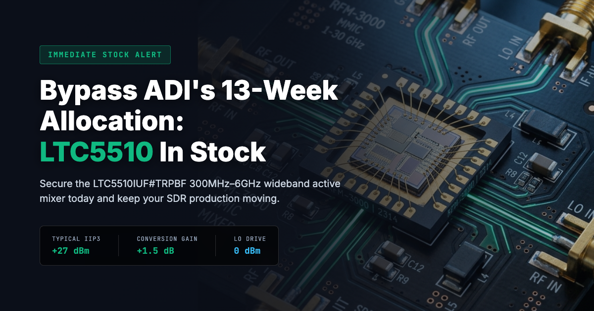
LTC5510IUF#TRPBF In Stock: Beat ADI's 13-Week Lead Time (≤70 chars)
LTC5510IUF#TRPBF Wideband Mixer Available Now: Beat the 13-Week Factory Lead Time on ADI's 300MHz–6GHz Active Mixer
Category: Hot Stock & Featured Parts | Author: Charles·Lee | Published: May 2026 | Last Updated: May 15, 2026
Key Takeaways:
- The Supply Chain Reality: In Q2 2026, Analog Devices (ADI) factory lead times for high-performance RF components have stretched past 13 weeks. For OEMs building 5G and SDR infrastructure, these delays are crippling product launch schedules and severely threatening quarterly revenue targets.
- The Silicon Masterpiece: The LTC5510IUF#TRPBF is an elite wideband active mixer capable of continuous operation from 300MHz to 6GHz. Its ability to function seamlessly as either an upconverter or downconverter allows hardware teams to massively consolidate their RF BOM, replacing a multitude of narrowband discrete mixers.
- Elite RF Performance: With a typical Input Third-Order Intercept (IIP3) of +27dBm, a conversion gain of +1.5dB, and an incredibly low 0dBm Local Oscillator (LO) drive requirement, the LTC5510 drastically simplifies LO generation circuitry, significantly lowers system power consumption, and completely eliminates the need for lossy IF amplification stages downstream.
- Immediate Availability: Forget the 13-week allocation queue. icallin has secured AS6081-verified, ready-to-ship inventory of the LTC5510, enabling immediate prototyping, pilot runs, and unhindered volume manufacturing.
- 📧 Submit an RFQ for the LTC5510 → — Secure your volume pricing immediately and keep your high-margin RF assembly line running without interruption.
1. Introduction — The RF Supply Chain Squeeze
The landscape of radio frequency (RF) engineering is currently undergoing a massive, fundamental architectural shift. The relentless global rollout of 5G Advanced infrastructure, the accelerated deployment of highly dense Low Earth Orbit (LEO) satellite internet constellations, and the urgent modernization of military Software Defined Radio (SDR) tactical platforms have collectively created an unprecedented surge in demand for ultra-wideband RF components. Hardware architects are rapidly abandoning traditional, narrow-band discrete radio signal chains in favor of highly integrated, frequency-agnostic front ends that can dynamically adapt to various communication protocols and spectrum allocations.
At the very heart of these modern, versatile RF front ends sits the active mixer—the most critical and arguably the most difficult-to-design component, responsible for accurately translating high-frequency RF signals down to manageable Intermediate Frequencies (IF) for digital processing, or translating synthesized IF signals up to transmission frequencies.
In this elite tier of RF silicon, the Analog Devices (formerly Linear Technology) LTC5510IUF#TRPBF is universally regarded as an industry benchmark. It represents the pinnacle of BiCMOS RF mixer design. However, its immense popularity among tier-1 telecommunications and aerospace contractors has created a severe supply chain bottleneck for the rest of the market.
As of Q2 2026, the global semiconductor market is experiencing significant structural constraints in specialized analog fabrication. ADI has recently announced targeted, systemic price increases (averaging roughly 15% across their high-performance RF and microwave catalog) designed to manage demand and offset rising wafer costs. But more critically for hardware developers, the factory lead times for the highly sought-after LTC5510 have stretched to an agonizing 13 weeks or beyond. For agile hardware teams operating on strict time-to-market deadlines, a 13-week delay for a single, irreplaceable BOM line item is absolutely catastrophic. A delayed product launch in the fast-paced 5G sector can result in permanently lost market share.
This article serves a critical dual purpose: first, to dissect the extraordinary RF engineering embedded within the LTC5510 silicon that makes it so indispensable to modern SDR design; and second, to provide procurement teams with a direct, immediate, and verified bypass to the ADI factory allocation queue via icallin's strategic stocking programs.
2. Unpacking the LTC5510IUF#TRPBF — Why it's Critical
To truly understand why OEMs and contract manufacturers are fiercely competing for LTC5510 inventory, we must dive deeply into the silicon's specifications. Designing a wideband mixer that maintains exceptional linearity, high conversion gain, and low noise across a multi-octave bandwidth is one of the most notoriously difficult challenges in analog Integrated Circuit (IC) design. The LTC5510 achieves this delicate balance with remarkable elegance, utilizing an advanced active mixer core topology.
Continuous Wideband Operation (300MHz to 6GHz)
Traditional, legacy RF mixers are inherently highly tuned "narrowband" devices, often relying on internal passive baluns that only operate efficiently over a small fraction of the spectrum. If an engineering team was building a multi-band cellular base station five years ago, they historically needed to qualify and source a specific discrete mixer for the 800MHz LTE band, another separate mixer for the 1.9GHz PCS band, and yet another mixer entirely for the 3.5GHz 5G NR band.
The LTC5510 completely obliterates this fragmented, multi-part requirement. It provides continuous, high-performance frequency translation capability from 300MHz all the way up to 6GHz. This massive bandwidth encompasses VHF, UHF, L-band, S-band, and C-band operations, entirely within a single, tiny 16-lead (4mm x 4mm) QFN package. This wideband capability allows engineers to design a single, universal hardware platform that can be software-configured to operate on virtually any commercial or tactical frequency.
Extreme Linearity (IIP3 and OIP3)
In modern dense RF environments—such as a crowded urban 5G small cell site or an active electronic warfare (EW) battlefield—the receiver antenna is constantly bombarded by strong out-of-band "blocker" signals adjacent to the desired weak signal. If the front-end mixer lacks sufficient linearity, these strong blockers will intermodulate within the mixer core, creating spurious intermodulation distortion (IMD) products that fold back into the desired IF band, completely crushing the receiver's sensitivity and dropping the communication link.
The LTC5510 boasts an exceptional Input Third-Order Intercept (IIP3) of +27dBm (typical at 2GHz) and an equally impressive Output Third-Order Intercept (OIP3). This extreme linearity ensures that the receiver can cleanly pluck a faint, microvolt-level signal out of a highly congested spectrum without suffering from distortion or desensitization. Achieving +27dBm IIP3 in an active mixer while maintaining reasonable DC power consumption is a testament to the underlying Linear Technology IP.
Conversion Gain vs. Conversion Loss
The vast majority of traditional passive diode-ring mixers suffer from significant conversion loss (typically ranging from -7dB to -9dB). This means the IF signal emerging from the mixer is roughly 8dB weaker than the RF signal entering it. To compensate for this loss, engineers are forced to cascade noisy, power-hungry, and space-consuming IF amplifiers downstream in order to recover the signal strength before feeding it to the Analog-to-Digital Converter (ADC).
The LTC5510 changes the paradigm because it is an active mixer topology. It actually provides a Conversion Gain of +1.5dB. By delivering a net signal gain rather than a loss, the LTC5510 inherently improves the overall cascaded Noise Figure (NF) of the entire receiver chain. Furthermore, this +1.5dB gain frequently allows engineers to completely eliminate one or more downstream IF amplifier stages, saving valuable PCB board space, reducing overall system power dissipation, and cutting significant BOM costs.
Zero-dBm LO Drive Requirement and Integrated Buffer
Generating a clean, ultra-low phase noise, high-frequency Local Oscillator (LO) signal is one of the most expensive and power-intensive aspects of radio design. Traditional high-linearity passive mixers require massive LO drive levels (often +15dBm to +17dBm) to switch the diode ring fully on and off. Driving an LO signal at +17dBm across a PCB requires dedicated, high-current RF buffer amplifiers, which consume tremendous amounts of DC power, generate significant thermal dissipation, and radiate severe Electromagnetic Interference (EMI) that can corrupt adjacent digital circuits.
The LTC5510 elegantly solves this by featuring a high-performance integrated LO buffer amplifier directly on the silicon die. Because of this internal amplification, the external interface requires an LO drive level of only 0dBm (typical). This ultra-low drive requirement allows the mixer to be driven directly by the output of a standard PLL/VCO synthesizer IC without needing any intermediate amplification, radically simplifying the LO generation network and preventing LO leakage across the board.
Table 1: LTC5510 Key RF Performance Specifications
| Performance Metric | LTC5510 Specification | Engineering Implication |
|---|---|---|
| RF Frequency Range | 300MHz to 6GHz | Covers almost all sub-6GHz commercial, IoT, and defense bands. |
| IIP3 (Linearity) | +27dBm (Typical) | Exceptional resistance to strong out-of-band blockers; prevents desensitization. |
| Conversion Gain | +1.5dB | Eliminates the need for lossy passive mixers and downstream IF recovery amps. |
| LO Drive Level | 0dBm (Typical) | Allows direct drive from a PLL/VCO; saves DC power, thermal budget, and PCB space. |
| Noise Figure (NF) | 11.6dB | Excellent sensitivity for an active mixer with such high IIP3, maximizing dynamic range. |
| Package | 16-Lead QFN (4mm x 4mm) | Ultra-compact footprint essential for dense phased-array and MIMO applications. |
Table 1: The core technical parameters that define the LTC5510's absolute dominance in the wideband active mixer market. | Source: ADI Datasheet | Compiled by: icallin.com
3. System Design: The SDR and 5G Application Advantage
The true, transformative value of the LTC5510 is fully realized when analyzing the system-level architecture. Modern RF engineering is defined by the Software Defined Radio (SDR) philosophy: designing a generic piece of highly capable hardware that can be reconfigured entirely via software to operate across vastly different frequency bands, channel bandwidths, and complex digital modulation schemes.
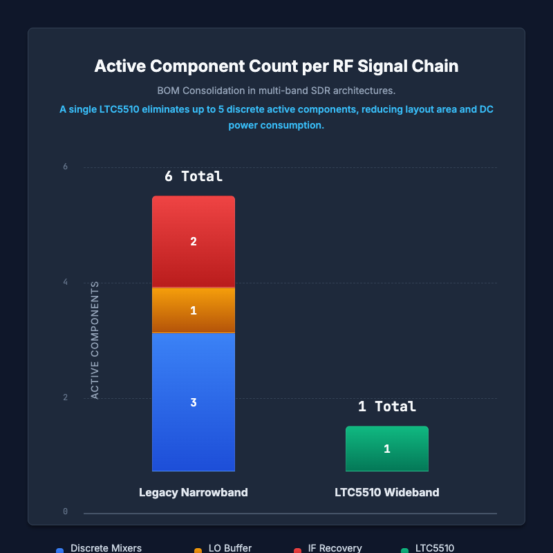
BOM Consolidation in SDR Architectures
In legacy hardware designs, creating a radio that could communicate on both a 400MHz military tactical band and a 2.4GHz commercial ISM band required two completely independent, parallel RF signal chains, complete with their own dedicated bandpass filters, Low Noise Amplifiers (LNAs), discrete mixers, and LO synthesizers.
With the LTC5510 acting as a universal, broadband upconverter or downconverter, the hardware architect can design a single, consolidated wideband RF front end. The incoming RF signal (regardless of frequency) is routed into the single LTC5510, and the system microcontroller simply commands the wideband LO synthesizer to change its frequency, instantly tuning the radio to a new band. This wideband consolidation strategy slashes the RF BOM count by up to 50%, significantly reduces the PCB area required, decreases SMT assembly failure rates by lowering component count, and dramatically lowers overall procurement complexity.
5G Sub-6GHz Cellular Base Stations and Massive MIMO
The aggressive global rollout of 5G New Radio (NR) networks in the highly coveted sub-6GHz spectrum relies almost entirely on Massive MIMO (Multiple Input, Multiple Output) active antenna units (AAUs). A single 5G macro cell might utilize 64 independent transmitter and receiver chains (a 64T64R configuration) to achieve the necessary spatial multiplexing and beamforming performance.
When an engineer is tasked with multiplying an RF circuit 64 times on a single, densely packed panel, DC power consumption and physical footprint become the absolute critical bottlenecks. The LTC5510's incredibly tiny 4mm x 4mm QFN package, combined seamlessly with its 0dBm LO drive requirement, makes it the perfect candidate for these extremely dense phased-array designs. The elimination of 64 discrete LO buffer amplifiers and 64 IF recovery amplifiers translates to massive thermal savings, allowing the 5G base station to operate reliably without massive active cooling systems.
Multi-Band Military Tactical Radios and Electronic Warfare
Defense contractors building man-pack tactical radios, vehicle-mounted SDRs, or airborne electronic warfare (EW) threat detection systems require hardware that is essentially "future-proof." The radio must possess the agility to rapidly scan, intercept, and transmit across an enormous swath of spectrum to evade hostile jamming attempts and establish secure, frequency-hopping communications.
The LTC5510's continuous 300MHz to 6GHz operational envelope ensures that whether the tactical radio is operating in legacy VHF/UHF bands for voice comms, or modern C-band frequencies for high-bandwidth drone video uplinks, the core frequency translation hardware remains robust, highly linear, and distortion-free.
Table 2: BOM Consolidation Analysis (Replacing narrowband mixers with the wideband LTC5510)
| Design Aspect | Legacy Narrowband Architecture | LTC5510 Wideband Architecture | The Consolidation Benefit |
|---|---|---|---|
| Mixer Count | 3 to 4 discrete mixers per board | 1 single LTC5510 per chain | Massive reduction in SMT placement cost, inventory tracking, and procurement risk. |
| LO Buffer Amps | Required (+15dBm drive minimum) | Eliminated (0dBm drive) | Saves >200mW of DC power per RF chain; drastically reduces EMI radiation. |
| IF Amplifiers | Required (to fix -8dB conversion loss) | Eliminated (+1.5dB conversion gain) | Removes noise-injecting active components from the highly sensitive IF path. |
| PCB Footprint | Large (Multiple segregated RF blocks) | Minimal (Single 4x4mm QFN) | Enables extremely dense 64T64R Massive MIMO array designs on small form-factor PCBs. |
Table 2: The profound system-level cost, power, and space savings achieved by adopting wideband active mixers in SDR architectures. | Source: icallin Engineering | Compiled by: icallin.com
4. Evaluation Boards — Accelerating Design via DC1983A and DC1984A
No seasoned RF engineer commits a highly complex active mixer to a custom PCB layout—especially a multi-layer board utilizing expensive high-frequency laminates like Rogers 4350B—without first exhaustively proving the concept in the lab. Analog Devices provides two excellent evaluation boards to radically accelerate this validation process: the DC1983A-F and the DC1984A-2-F.
The DC1983A-F (Downconverter Evaluation)
The DC1983A-F is factory-configured to test the LTC5510 specifically in a receiving (downconverting) application. While the LTC5510 silicon is inherently wideband, elite RF engineers understand that to achieve the absolute maximum dynamic range and optimal power transfer (lowest VSWR) at a specific target frequency, the RF input port and IF output port must be finely tuned with a passive LC impedance matching network.
The DC1983A-F evaluation board is designed with easily accessible 0402 component pads, allowing engineers to quickly swap out surface-mount inductors and capacitors using a soldering iron. This enables them to dial in the perfect, conjugate impedance match for their specific 5G or SDR band, observing the exact IIP3, conversion gain, and Noise Figure on their vector network analyzers (VNAs) and spectrum analyzers long before they begin drawing schematics in their CAD software.
The DC1984A-2-F (Upconverter Evaluation)
Conversely, the DC1984A-2-F is specifically configured to evaluate the LTC5510 as an upconverter in a transmitter chain. In a transmitting application, the critical metrics shift slightly; engineers are heavily focused on the Output 1dB Compression Point (P1dB), out-of-band spurious emissions, and LO-to-RF leakage suppression. The board provides high-quality, high-frequency SMA connectors to easily inject the baseband/IF signal and cleanly monitor the resulting high-frequency RF output, ensuring the transmitted spectrum complies with strict FCC or ETSI regulatory masks.
The Prototype-to-Production Chasm
The single greatest tragedy in modern hardware development is an engineering team flawlessly executing their evaluation phase, finalizing a beautiful PCB layout, spinning their first pilot run, and then discovering that the silicon they just designed their entire product around has suddenly entered allocation with a 13-week factory lead time.
This scenario represents the dreaded "Prototype-to-Production Chasm." icallin bridges this chasm by aligning our strategic inventory specifically with the engineering lifecycle. By stocking bulk quantities of the LTC5510IUF#TRPBF, we ensure that the exact silicon you validated on the DC1983A evaluation board is available for immediate, overnight shipping the precise moment your pilot-run PCBs arrive from the fabrication house. We guarantee that your transition from lab prototype to volume production is seamless and uninterrupted.
5. Market Dynamics: Price Hikes, Allocation, and 13-Week Lead Times
Engineering elegant SDR solutions is a tremendous achievement, but it is only half the battle; navigating the volatile, unpredictable semiconductor supply chain is the other, equally critical half. In 2026, the market dynamics surrounding high-performance analog and RF Integrated Circuits are particularly hostile to agile manufacturing and just-in-time (JIT) procurement models.
The ADI Pricing and Allocation Squeeze
Early in Q1 2026, Analog Devices initiated a broad, strategic pricing adjustment across their portfolio. They raised prices significantly on older generation legacy parts to aggressively incentivize migration to newer architectures, while simultaneously applying a ~15% premium to high-demand, high-performance silicon like the LTC5510 to offset rising foundry costs.
Furthermore, the manufacturing reality is that wideband active mixers utilize highly specialized Silicon-Germanium (SiGe) BiCMOS fabrication processes. These advanced RF processes cannot be easily offloaded or outsourced to standard digital CMOS foundries (like TSMC or GlobalFoundries) when demand spikes. Consequently, capacity is rigidly fixed. As massive defense contractors and global telecommunications giants consume massive volumes of these chips for strategic satellite constellations and 5G network build-outs, mid-tier OEMs are inevitably relegated to the back of the factory allocation queue, facing standard lead times of 13 weeks or significantly longer.
The Mathematics of Opportunity Cost
When an OEM procurement manager is faced with a 13-week lead time on a $15 RF mixer, they must step back and calculate the true, holistic cost of that delay. If a company manufactures a high-end SDR tactical platform that sells for $5,000, and their entire production line is halted for 3 months because they lack the LTC5510, the financial hemorrhage is staggering. They face lost revenue, missed contractual milestones, idle factory overhead, and severe damage to their brand reputation.
In this stark context, securing immediate, verified inventory from an independent, highly credentialed stocking distributor like icallin—even if current market dynamics dictate a slight spot-market premium—is absolutely not an expense; it is a critical Return on Investment (ROI) safeguard. Paying an extra $5 for a component today to unlock a stalled $5,000 product shipment tomorrow is the very definition of sound, strategic procurement. It transforms a supply chain crisis into a competitive advantage.
Mitigating Severe Counterfeit Risks in the Gray Market
The secondary electronic components market is acutely aware of the massive demand and severe shortage of the LTC5510. Unscrupulous gray market brokers frequently attempt to exploit this desperation by selling "factory reject" silicon that failed ADI's stringent internal linearity tests, or by re-marking lower-tier, cheaper mixers with counterfeit LTC5510 laser etchings.
In a high-frequency RF circuit, a counterfeit or substandard mixer will immediately manifest as catastrophic noise figure degradation, linearity collapse (poor IIP3), or massive LO leakage, completely ruining the final product and causing it to fail FCC/CE compliance testing.
To navigate this treacherous landscape, procurement managers must strictly utilize distributors with AS6081 certification and rigorous in-house testing capabilities. They must ensure that every single reel of LTC5510 entering their facility is pristine, traceable, and undeniably authentic.
Table 3: 2026 RF Mixer Supply Chain ROI Matrix (Lead Time vs. Opportunity Cost)
| Supply Source | Current Lead Time | Risk Profile | ROI Impact on Stalled Production |
|---|---|---|---|
| Factory Direct (Allocation) | 13 to 26 Weeks | Very Low (Authentic) | Catastrophic (Missed market windows, halted revenue, delayed launches). |
| Unverified Gray Market | Immediate | Extremely High (Counterfeits) | Severe (Massive RMA costs, brand damage, failed RF compliance testing). |
| icallin Verified Stock | Immediate (5-7 Days) | Very Low (AS6081 Tested) | Optimal (Production resumes immediately, revenue unlocked, market share gained). |
Table 3: Strategic procurement mapping for high-value ADI RF components during structural, industry-wide shortages. | Source: icallin Market Intelligence | Compiled by: icallin.com
6. icallin’s Inventory Advantage
At icallin, we do not simply react to shortages; we anticipate them. We utilize advanced predictive analytics, deep industry relationships, and market intelligence to monitor global supply chain bottlenecks before they paralyze the market. Recognizing the absolutely critical importance of the LTC5510 to the rapidly expanding SDR, 5G, and defense sectors, we proactively secured bulk, authentic inventory long before the current 13-week allocation crunch fully materialized.
Immediate Global Dispatch Without Excuses
We are not brokers, and we do not deal in "ghost inventory." The LTC5510IUF#TRPBF reels listed on our platform are physically residing in our environmentally controlled, ESD-safe warehouses right now. When an OEM issues an urgent RFQ to resolve a line-down situation, we execute rapid, precise fulfillment. Both domestic and international shipments are typically dispatched and delivered within 5 to 7 days via fully compliant, secure logistics partners (DHL, FedEx, UPS).
Uncompromising Quality Assurance Protocols
Because RF silicon is hyper-sensitive to both Electrostatic Discharge (ESD) handling and environmental moisture degradation, our inventory management protocols are draconian. Every single reel of LTC5510 undergoes strict AS6081-compliant visual and microscopic inspection, ensuring pristine solder contacts, flawless moisture barrier bagging (MBB), intact humidity indicator cards (HIC), and absolute traceability back to the original manufacturing lot.
Your Strategic Supply Chain Buffer
icallin acts as the ultimate shock-absorber for your highly sensitive RF supply chain. Whether your engineering team needs a small cut-tape quantity of 50 pieces to populate a handful of DC1983A evaluation boards for an initial pilot run, or a full factory-sealed reel to keep your 5G base station SMT line running through the weekend, our inventory represents your immediate, guaranteed bypass to the ADI factory allocation queue.

Frequently Asked Questions
Q1: Can the LTC5510 truly operate at 300MHz and 6GHz simultaneously without changing the circuit board?
The internal active mixer core of the LTC5510 is inherently wideband. However, to achieve the absolute optimal RF power transfer (the lowest possible VSWR and insertion loss) into and out of the chip, the external passive matching components (the inductors and capacitors at the RF and IF ports) must be tuned to a specific, narrower frequency band. You can absolutely design a "compromise" broadband match that works across the entire range, but be aware that it will slightly degrade the absolute peak IIP3 and Noise Figure performance compared to a narrowly tuned, band-specific match.
Q2: Why does the LTC5510 have such a uniquely low LO drive requirement (0dBm)?
Unlike traditional passive diode-ring mixers, the LTC5510 features a high-performance integrated Local Oscillator buffer amplifier situated directly on the silicon die. This internal buffer takes the relatively weak 0dBm signal generated by your external PLL/synthesizer and internally amplifies it to the massive voltage swings required to rapidly switch the active mixer core. This brilliant integration saves you the immense trouble, cost, and PCB space of designing discrete, high-power external LO amplifiers.
Q3: Is the LTC5510 classified as an active or passive mixer?
It is an active mixer topology. This is precisely why it provides a Conversion Gain (typically +1.5dB) rather than suffering from a Conversion Loss (like the -8dB seen in passive mixers). The active transistor circuitry also provides vastly superior isolation between the RF, LO, and IF ports, preventing signals from leaking backwards through the system.
Q4: Are the ADI evaluation boards (DC1983A and DC1984A) also facing severe shortages?
Evaluation board availability fluctuates heavily and is often independent of the raw silicon supply. While we deeply stock the bare silicon chips (LTC5510IUF#TRPBF), hardware teams can often successfully secure the necessary EVBs through standard distribution channels (like DigiKey or Mouser) or directly from ADI to begin their lab software integration, while simultaneously securing the actual production silicon from icallin to ensure their manufacturing run is protected.
Q5: How do I verify the absolute authenticity of icallin’s LTC5510 stock?
We adhere strictly to AS6081 anti-counterfeit standards. All incoming inventory is subjected to rigorous, multi-point inspection. Upon request, we provide comprehensive, high-resolution photographic evidence of the reels, factory labels, lot codes, and moisture indicator cards prior to shipment, giving your quality assurance team complete confidence in the product's pedigree.
Conclusion
The Analog Devices LTC5510IUF#TRPBF is an undeniable masterclass in high-frequency RF engineering. By offering continuous 300MHz to 6GHz operational bandwidth, extreme linearity (+27dBm IIP3), and a highly integrated active design that eliminates the need for external IF and LO amplifiers, it stands as the cornerstone component for any modern Software Defined Radio, LEO satellite terminal, or 5G platform.
However, the brutal reality of the 2026 semiconductor supply chain is that a vastly superior schematic cannot compensate for an empty stockroom. A 13-week lead time is an unacceptable, existential risk for agile OEMs seeking to dominate the telecommunications market.
By leveraging icallin’s rigorously verified, ready-to-ship inventory, engineering and procurement teams can seamlessly transition from prototyping on the DC1983A evaluation board to full-scale volume manufacturing without missing a single, critical beat. Stop waiting endlessly in the factory allocation queue. Secure your wideband active mixers today, guarantee your revenue stream, and keep your RF assembly line moving at full speed.
📧 Submit an RFQ for the LTC5510IUF#TRPBF →
Related Internal Resources
- ADI LTC5510IUF#TRPBF — Product Detail
- Analog Devices (ADI) Manufacturer Page
- RF/Microwave Component Category
- Submit RFQ
*Charles·Lee is a Senior Procurement Specialist and RF Supply Chain Analyst at icallin.com. With a profound understanding of Software Defined Radio architectures and volatile semiconductor market dynamics, Charles specializes in securing hard-to-find, high-performance analog and RF components for Tier-1 defense and telecommunications OEMs worldwide.

Top Recommended part