Copper-Clad Laminate Sets the PCB’s Electrical and Mechanical Baseline
Copper-Clad Laminate Sets the PCB’s Electrical and Mechanical Baseline
Copper-clad laminate, usually shortened to CCL, is the starting sheet from which PCB conductors and structural layers are made. It combines copper foil with an insulating laminate so the same material system must support imaging and etching, carry mechanical loads, separate conductors, and preserve electrical behavior through fabrication and service.
That makes copper clad laminate selection an early design decision, not a line item to leave until a board is quoted. The exact dielectric system, reinforcement, copper foil, thickness, surface treatment, and qualification define a baseline that later routing cannot repair. A well-routed design can still miss loss, impedance, flatness, thermal, or reliability targets if its assumed laminate does not match the buildable material.
What Copper-Clad Laminate Contains
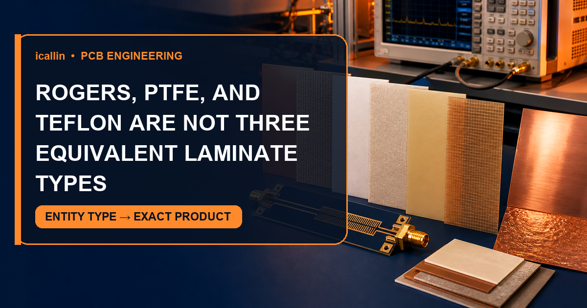
A conventional rigid CCL consists of a cured resin-and-reinforcement laminate faced with copper foil on one or both sides. Woven glass with epoxy resin is common, but low-loss hydrocarbon systems, PTFE-based materials, polyimide constructions, paper or composite reinforcements, and insulated metal substrates serve different applications. Flexible copper-clad materials may use polyimide or another flexible dielectric and can be adhesive-based or adhesiveless.
The term describes a product form, not one chemistry. Two sheets sold as CCL can differ in dielectric behavior, copper profile, glass style, thermal expansion, moisture response, flame performance, and process requirements. A specification must therefore identify the qualified material and copper construction rather than relying on “CCL” or “FR-4” alone.
CCL is also not a finished PCB. Fabrication removes selected copper to form traces and planes, drills or lasers holes, prepares hole walls, plates conductive features, applies surface finish and solder mask, profiles the board, and performs inspection and test. The starting laminate influences every one of those operations, but it does not contain the finished interconnect by itself.
The Copper Foil Is Part of the Laminate Decision
Copper provides the conductive surface that will become pads, traces, and planes. Thickness affects conductor resistance, current density, thermal spreading, etch geometry, minimum spacing, and controlled impedance. Outer-layer finished copper can include later plating, so incoming foil thickness and finished thickness should not be treated as identical values.
Foil profile and treatment help bond copper to the dielectric. That bond must survive processing and service, yet roughness can increase conductor loss as frequency rises. Low-profile foils can benefit demanding channels, but they still require a compatible laminate interface and verified adhesion. Rolled and electrodeposited foils are available in multiple treatments and weights; the production method alone does not guarantee flexibility, smoothness, or high-frequency performance.
The Dielectric Establishes the Electrical Baseline
Dielectric constant influences propagation velocity and the geometry needed for a target impedance. Dissipation factor contributes to dielectric loss, while conductor roughness, trace dimensions, discontinuities, and route length contribute additional loss. Lower Dk does not automatically mean lower loss, and one catalog Dk cannot be moved between test methods or frequencies without review.
For controlled impedance or phase-sensitive routing, use the material supplier's relevant design data and the fabricator's actual core thickness. Include copper profile and thickness tolerance in the interconnect model. A generic material family may be acceptable for an early estimate, but production release should be tied to an approved stackup and an alternate-material rule that preserves the required electrical properties.
The Same Sheet Carries Mechanical and Thermal Loads
CCL supports the board through drilling, assembly, connector insertion, mounting, vibration, and thermal cycling. Finished thickness, flexural behavior, dimensional stability, warpage, and copper balance all contribute. A thicker sheet may be stiffer, but it does not automatically improve heat removal, trace current capacity, impedance control, or voltage safety.
Thermal review should separate resin transition, decomposition resistance, expansion, and heat conduction. Tg identifies a transition in resin behavior, not a continuous-use ceiling or melting point. Z-axis expansion is important to plated-hole reliability, while in-plane movement affects registration. Thermal conductivity matters to a heat path, but copper planes, vias, interfaces, mounting, airflow, and the final heat sink still determine component temperature.

CCL Families Solve Different Problems
| CCL family | Typical design reason | Critical checks |
|---|---|---|
| Epoxy-glass rigid laminate | General rigid and multilayer circuitry | Exact Dk/Df, Tg method, CTE, moisture, copper profile, thickness tolerance |
| Low-loss or PTFE-based laminate | RF, microwave, antenna, or long high-speed channels | Design Dk, loss, foil roughness, dimensional stability, drilling and bonding process |
| Polyimide flexible laminate | Static bends, dynamic flex, or rigid-flex transitions | Adhesive system, copper type, bend construction, moisture, dimensional movement |
| Insulated metal laminate | A short thermal path from selected power devices to a metal base | Dielectric thermal resistance, isolation, copper layout, interface and mounting |
Table 1: CCL families are compared by the requirement they solve, not by a universal performance ranking.
FR-4 remains a practical default for many rigid boards, but it is a broad family rather than a single property set. A low-loss CCL is justified when the modeled and measured channel requires it. Flexible material is selected when the interconnect must bend as a designed structure. A metal-base construction helps only when its dielectric and interfaces create a useful thermal path. None of these categories is automatically “best.”
How CCL Is Made—and Why Process Compatibility Matters
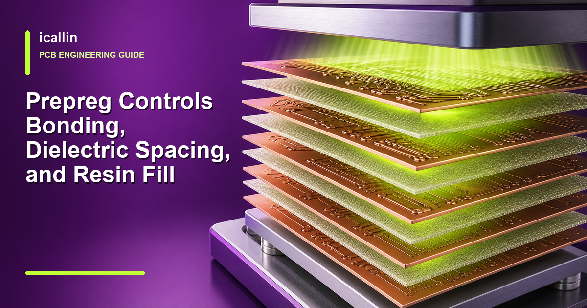
At a high level, reinforcement is combined with a controlled resin system, advanced to the required cure state, stacked with copper foil, and consolidated under a qualified temperature-and-pressure cycle. The cured sheet is cooled, trimmed, inspected, and prepared for shipment. Flexible adhesiveless materials and specialty thermoplastic or thermoset systems use different routes, so one generic process description should not be imposed on every CCL.
PCB fabrication later exposes the material to imaging, etching, oxide or alternative surface preparation, lamination, drilling, desmear, plating, soldering, and cleaning. A laminate chosen only for a favorable Df or Tg can fail the project if the selected fabricator cannot process it within an approved window. Material availability should be discussed together with core thicknesses, prepregs or bondplies, copper foils, drill behavior, registration, and acceptable substitutions.
What to Put in a CCL Selection Record
Begin with the application requirements: impedance and loss budget, voltage, finished thickness, copper by layer, mechanical support, assembly profile, service temperature, moisture, chemicals, flexing, and intended life. Translate those needs into properties that can be compared with conditions attached.
Record the exact laminate product or governing specification, core thickness and tolerance, copper foil weight and profile, Dk/Df data and test context, Tg test method, Z-axis CTE, decomposition or delamination indicators, moisture behavior, dimensional stability, flammability or safety requirements, and surface quality criteria. Visual defects such as wrinkles, dents, pinholes, exposed reinforcement, or resin anomalies require defined acceptance rules rather than an informal “looks good” standard.
Then confirm that the complete stackup is available and qualified at the selected board house. If alternates are allowed, define the minimum electrical, thermal, mechanical, copper, and process equivalence required. A purchasing description such as “high-Tg FR-4” is too broad to protect a controlled-impedance or high-reliability design.
Frequently Asked Questions
Is copper-clad laminate the same as a finished PCB?
No. CCL is the copper-faced insulating sheet used as a starting material. PCB fabrication patterns the copper, creates and plates holes, adds other layers where required, applies finishes and protective coatings, profiles the outline, and tests the finished interconnect. The CCL establishes important material boundaries, but it is only one input to the completed board.
Does a lower dielectric constant always make a CCL better for high-speed signals?
No. Dk affects impedance geometry and propagation velocity, while Df, copper roughness, route length, glass structure, temperature, moisture, and discontinuities contribute to total channel behavior. The useful material is the one that meets the modeled loss, phase, impedance, thermal, mechanical, and fabrication requirements with controlled data—not simply the lowest Dk number.
Conclusion
Copper-clad laminate is the physical and electrical baseline beneath every later PCB operation. Its copper foil defines conductor starting conditions; its dielectric controls spacing, insulation, and part of the signal behavior; and its cured structure supports drilling, assembly, and service loads.
Select CCL by the complete application and manufacturing problem. Preserve the test conditions behind property values, specify the copper and core construction, confirm a qualified fabrication route, and control substitutions. Doing that before routing begins prevents the starting material from becoming an expensive late-stage variable.
Need Help With PCB Manufacturing or PCBA Assembly?
Share your PCB manufacturing or PCBA assembly requirements with icallin through our dedicated quotation page.