PCB Copper Thickness: Current, Etching, and Impedance
Copper Thickness Changes Current, Etching, and Impedance at Once
PCB copper thickness is not an isolated order option. Changing it alters conductor resistance and temperature rise, the amount of copper that must be etched, the minimum practical line and space, and the geometry used to calculate impedance. A useful selection therefore solves all four constraints at the same time.
The familiar labels—0.5 oz, 1 oz, 2 oz, and heavier copper—are convenient starting points, not complete finished-conductor specifications. Designers must distinguish nominal foil weight from base copper, plated outer-layer copper, and the final cross-section that the fabricated trace will actually have.
Copper Weight Is Areal Mass, Not a Direct Length Unit
In PCB terminology, “1 oz copper” means a nominal ounce of copper distributed over one square foot. Converting that areal mass with copper density gives a thickness of roughly 34–35 µm, commonly rounded to 35 µm or about 1.37 mil. The shorthand is useful, but foil tolerances, surface profile, etching, and plating prevent it from being an exact measurement of every finished trace.
| Nominal copper weight | Common metric shorthand | Approximate mil value | Typical design context |
|---|---|---|---|
| 0.25 oz/ft² | 9 µm | 0.35 mil | Very fine features or selected build-up layers |
| 0.5 oz/ft² | 17–18 µm | 0.7 mil | Fine-line inner layers and some signal layers |
| 1 oz/ft² | 34–35 µm | 1.35–1.38 mil | General-purpose signal, ground, and power layers |
| 2 oz/ft² | 68–70 µm | 2.7–2.8 mil | Higher-current paths and added heat spreading |
| 3 oz/ft² | 102–105 µm | 4.0–4.1 mil | Heavy-copper constructions with coarser features |
Table 1: Values are nominal conversions; purchasing and acceptance must use the fabricator's defined foil and finished-copper tolerances | Compiled by: icallin.com
A mathematically precise conversion does not eliminate specification ambiguity. “One ounce finished” may mean something different from “one ounce base foil” at a particular board shop. Write the intended finished copper requirement by layer and confirm how the fabricator builds it.
Base Copper, Plating, and Finished Copper Are Different
Inner layers of a conventional multilayer board are usually imaged and etched from copper-clad cores. Their final conductor thickness is therefore closely related to the starting foil, with etch profile and process tolerance included.
Outer layers commonly start with thinner base foil and receive additional copper during through-hole and pattern plating. The amount deposited across traces, pads, hole walls, and panel locations is not perfectly uniform. A nominal starting foil alone therefore cannot describe the completed outer conductor. Surface finishes such as ENIG or immersion silver add other metals on exposed pads but are not part of the copper thickness.
Common verification methods answer different questions. Foil weight can be checked by mass per area. A polished microsection shows the local conductor and hole-wall cross-section. A profilometer can measure a surface step under controlled conditions. Acceptance sampling, location, preparation, and measurement method should match the applicable drawing and performance specification.

Effect 1: Current Capacity Depends on the Whole Thermal System
For a trace of fixed length and width, increasing copper thickness increases cross-sectional area and lowers DC resistance. The basic relationship is:
R = ρL / (w × t)
where ρ is copper resistivity, L is trace length, w is width, and t is finished thickness. Lower resistance reduces I²R loss at a given current, but it does not assign a universal ampere rating to an ounce value.
Allowable current depends on permitted temperature rise, trace width and length, whether the conductor is on an external or internal layer, nearby copper planes, dielectric construction, airflow, enclosure temperature, duty cycle, via transitions, neck-downs, terminals, and assembly limits. IPC-2152 provides a thermal-design framework, while simulation or measurement may be warranted for dense power electronics.
Check the narrowest and hottest part of the path. A wide 2 oz pour does not help if current must pass through a small pad, a thin spoke, one via, or a connector pin. Similarly, adding copper can spread heat across the board, but the heat still needs a path to air, a chassis, or a heatsink.
Effect 2: Thicker Copper Pushes Against Fine Lines and Spacing
Subtractive etching removes copper downward through the foil and laterally beneath the resist. A thicker layer needs a deeper etch, so controlling sidewall undercut and the final trapezoidal trace profile becomes harder. Fabricators compensate in imaging and process control, but thicker copper generally requires wider minimum conductors and larger gaps than thinner copper.
There is no universal line/space value for each ounce. Etchant chemistry, equipment, imaging process, panel density, copper distribution, starting foil, plating sequence, and the board shop's control plan all matter. Use the fabricator's current capability table for the selected layer type and copper construction, then leave margin instead of routing at an advertised limit everywhere.
This tradeoff can force an architectural decision. A power rail may be better split across parallel planes, moved to a less congested layer, reinforced with multiple vias, or widened locally rather than making every layer heavy copper and sacrificing escape routing for fine-pitch components.
Effect 3: Copper Thickness Changes Controlled Impedance
Trace impedance is set by the electromagnetic field around the conductor, not by width alone. For a microstrip or stripline, the field depends on dielectric height, material Dk, trace width, finished copper thickness, etched sidewall shape, reference-plane geometry, and—on outer layers—the solder-mask coating. Edge-coupled differential pairs also depend on pair spacing.
With width and dielectric geometry held constant, increasing trace thickness generally lowers characteristic impedance because the conductor presents a larger field boundary. The correction is not safely handled by scaling width with a simple rule. A field solver should use the approved stackup, finished outer-layer plating, expected trapezoidal cross-section, and material design values.
This is why changing from 1 oz to 2 oz after routing can invalidate both the impedance calculation and the manufacturability check. The solver may call for a narrower trace or different pair spacing just as the thicker copper makes narrow etched features harder to produce. Resolve that conflict with the fabricator before the stackup and routing are frozen.
At high frequency, conductor surface profile adds another variable. Current crowds toward the conductor surface, and rough foil can increase insertion loss. Nominal copper weight does not reveal that roughness, so loss-sensitive designs should specify a compatible foil profile and laminate construction as well as thickness.
Layer Count Does Not Dictate Copper Weight
Multilayer boards often use different copper weights on inner and outer layers, but there is no rule that adding layers requires heavier copper or a higher-Dk dielectric. Layer count, copper thickness, dielectric spacing, and material Dk are independent stackup choices that must be solved together.
Thin inner copper can make dense routing easier, while selected power layers may use heavier copper. Outer-layer thickness is influenced by hole plating. Dielectric spacing is then chosen to meet total board thickness, resin-fill, voltage, coupling, and impedance requirements. Higher Dk is not automatically better insulation, and more total copper does not guarantee lower component temperature.
Copper Balance and Pours Still Need Electrical Review
Large differences in copper coverage can affect plating, etching, resin flow, local thickness, and board flatness. Designers and fabricators may use balancing features or panel thieving to make processing more uniform. Those additions must preserve clearance, creepage, antenna keepouts, and controlled-impedance fields.
A copper pour is not automatically a useful ground plane. It must be assigned to the correct net, remain continuous, and connect through adequate vias where return current changes layers. Floating islands or narrow branches can couple to signals, create resonances, or undermine the intended return path. Copper added for process balance should never be assumed electrically invisible.
A Selection Workflow That Avoids Late Surprises
- Define the electrical load. Record current, duty cycle, route length, acceptable voltage drop, and permitted temperature rise for every high-current path.
- Choose a candidate layer construction. State base and finished copper by layer, including the fabricator's expected outer-layer plating.
- Check current and temperature. Use an IPC-2152-based method, a validated calculator, simulation, or test data appropriate to the geometry and environment.
- Check etching and spacing. Compare every trace, gap, pad, annular ring, and fine-pitch escape against the fabricator's rules for that copper thickness.
- Recalculate impedance. Use finished trace thickness, dielectric geometry, Dk, solder mask, pair spacing, and etch profile in a field solver.
- Confirm the approved stackup. Align copper tolerances, material choices, impedance coupons, measurement method, and any substitutions before release.
- Verify the finished board. Use coupons, resistance checks, microsections, impedance testing, and thermal measurement in proportion to product risk.
The order is intentionally iterative. If thicker copper fixes temperature rise but breaks fine-pitch spacing or impedance geometry, revisit width, layer assignment, parallel paths, via count, cooling, or the board architecture rather than accepting a hidden compromise.
Conclusion
Copper weight is a convenient purchasing language, but finished geometry is what the circuit experiences. About 1 oz/ft² corresponds to roughly 34–35 µm of nominal foil; outer-layer plating, etching, and process tolerances then shape the actual conductor.
Choose thickness with current, temperature rise, trace width, etch capability, spacing, and controlled impedance open at the same time. Document the construction by layer and confirm it with the fabricator. That approach turns “1 oz or 2 oz?” from a checkout-box decision into a controlled electrical and manufacturing choice.
Need Help With PCB Manufacturing or PCBA Assembly?
Share your PCB manufacturing or PCBA assembly requirements with icallin through our dedicated quotation page.


Related Blogs
View All Blogs
PCB Thickness for Connector and Enclosure Interfaces
Define PCB thickness from card-edge connector and enclosure limits, then fit stackup, tolerance, drilling, and inspection inside the fixed mechanical envelope.

Finished PCB Thickness: Specify Tolerance and Acceptance
Define finished PCB thickness with a nominal value, tolerance, stackup scope, measurement method, sampling plan, and connector or enclosure acceptance limits.
Rogers vs PTFE PCB Laminates: Understand the Difference
Separate Rogers product families, PTFE polymers, and the Teflon brand, then compare exact laminate Dk, Df, copper, thermal, mechanical, and process data.

Flex PCB Materials Must Survive Bending, Heat, and Assembly
Choose flexible PCB materials by bend duty, assembly heat, electrical loss, moisture, adhesive system, coverlay, and validated fabrication limits.

PCB Laminate Selection Must Include the Lamination Process
Match PCB laminate materials to resin flow, surface preparation, pressure, temperature, and cure windows to reduce voids, delamination, and registration risk.
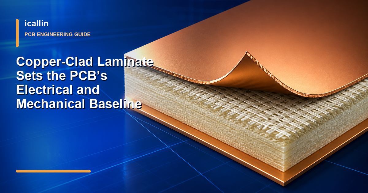
Copper-Clad Laminate Sets the PCB’s Electrical and Mechanical Baseline
Choose copper-clad laminate by dielectric system, copper foil, Dk/Df, thermal expansion, thickness, flatness, and processing needs before routing begins.