Flex PCB Materials Must Survive Bending, Heat, and Assembly
Flex PCB Materials Must Survive Bending, Heat, and Assembly
Flexible PCB material selection is a system decision, not a choice of base film alone. The substrate, copper, bonding layer, coverlay, stiffeners, surface finish, and assembly process must work together through installation, soldering, temperature exposure, and the required number of bends.
A material that has attractive dielectric data can still fail if its copper construction cracks at the bend, its adhesive absorbs moisture, or its coverlay opening concentrates strain beside a solder joint. Start with the mechanical duty and assembly profile, then narrow the electrical and environmental options.
Define the Flexing Duty Before Comparing Materials
The word flexible covers several different operating conditions. A static-flex circuit bends during installation and then remains in place. A dynamic-flex circuit moves repeatedly in service, as in a hinge, printhead, or moving sensor. A flex-to-install design may experience only a few controlled folds but can still be damaged by a sharp crease or an assembly fixture.
Record the minimum bend radius, bend angle, active bend length, cycle count, motion speed, temperature range, and whether the same area twists as well as bends. Also mark component zones, stiffener transitions, connector interfaces, and any location where the circuit will be clamped. These constraints determine whether a thin adhesiveless construction is worth its cost, where neutral-axis control matters, and how much copper and coverlay can safely pass through the moving region.
No generic bend-radius multiplier proves reliability. The permitted radius depends on the complete stack, copper type and thickness, layer count, coverlay, adhesive, conductor direction, and whether movement is static or dynamic. Use the applicable flex-design rules and validate the production construction under the real motion profile.
Choose the Substrate for the Actual Environment
Polyimide is the common starting point for many flexible circuits because it combines useful thermal endurance, dielectric behavior, chemical resistance, and dimensional stability. It is available in many thicknesses and constructions, but “polyimide” is still a material family. Film grade, treatment, thickness, and the chosen adhesive system affect the final circuit.
Polyester films such as PET can be attractive for cost-sensitive, low-stress products that use a compatible low-temperature assembly process. They should not be selected from price alone. The designer must confirm soldering or interconnection temperature, dimensional change, chemical exposure, expected flex life, and the temperature range of the finished product.
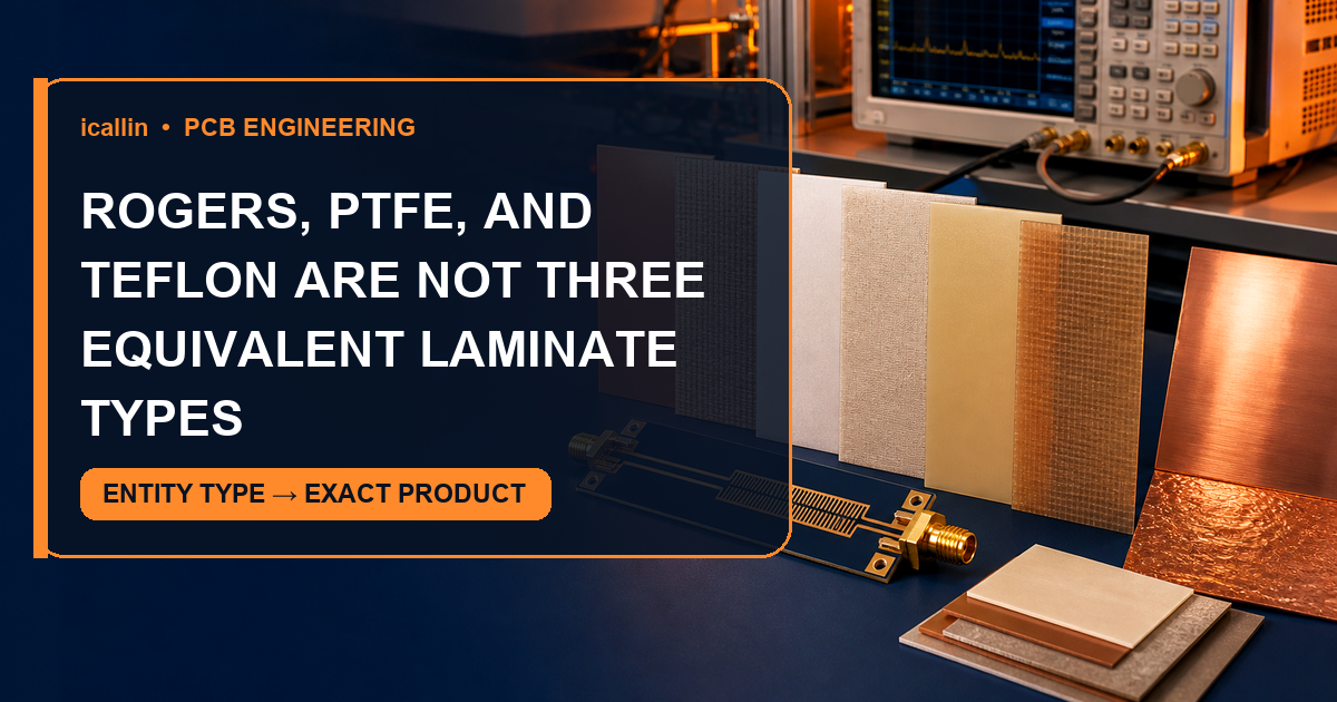
Liquid-crystal polymer can be useful where low moisture uptake, dimensional control, or high-frequency performance matters. PTFE-based constructions can serve specialized low-loss or chemically demanding circuits, but they are not automatic replacements for conventional flex materials. Both categories require exact laminate data and a fabricator experienced with the selected construction.
The safest comparison uses the exact film or laminate data sheet, not a generic material label. Check thickness tolerance, in-plane dimensional behavior, dielectric constant and dissipation factor at the relevant test method and frequency, moisture response, thermal cycling, flammability requirement, and compatibility with the intended bonding and cover systems.
Copper Often Controls Flex Life
Copper is both the conductor and a major mechanical member of the flex stack. Thinner copper generally reduces bending strain, but current, voltage drop, etching, and connector requirements may set a lower limit. Rolled-annealed copper is often considered for dynamic flex because its grain structure can support repeated bending better than some electrodeposited foils, yet the exact foil grade and processing history still matter.
Trace geometry can be more important than a small change in base-film properties. Keep conductors perpendicular to the bend axis where practical, avoid sharp corners, stagger features between layers, and prevent abrupt width changes in the active bend. Solid copper areas, hatched planes, vias, plated holes, and component pads need deliberate placement because each changes local stiffness and strain.
For multilayer flex, balance copper and dielectric construction around the neutral axis. Adding layers, thicker copper, shielding films, or stiffeners can move the neutral axis and increase strain in a critical conductor. Model the actual stack rather than treating the substrate thickness as the entire mechanical section.

Adhesive and Adhesiveless Constructions Change the Stack
Bonding films attach copper, coverlay, and stiffeners. Acrylic systems are widely used where flexibility and adhesion are important; epoxy systems can offer a different balance of thermal, chemical, and mechanical behavior. Exact performance varies by formulation and thickness, so a generic temperature statement is not a purchasing specification.
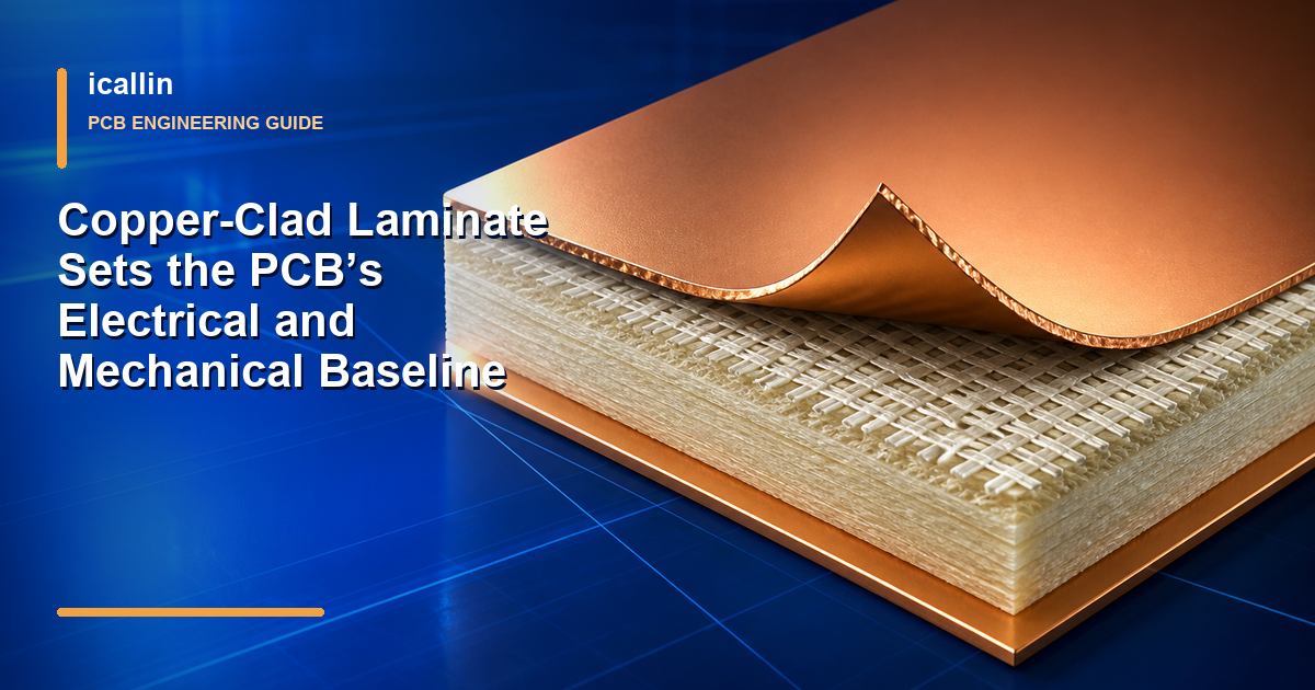
Adhesiveless copper-clad film removes a separate substrate-to-copper adhesive layer. This can reduce thickness, improve dimensional control, and simplify strain management in fine-feature or dynamic-flex designs. It does not remove every adhesive from the circuit: coverlay and stiffener attachment may still use bonding films. It can also change material cost and fabrication options.
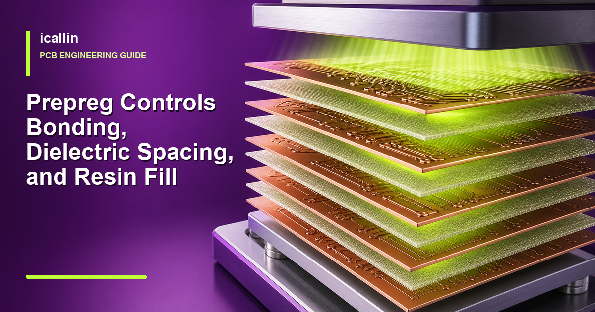
Resin flow at coverlay openings and stiffener edges deserves attention. Excess adhesive can encroach on pads, while insufficient flow can leave voids or weak edges. The fabricator's controlled lamination process, artwork compensation, and inspection criteria must match the chosen material set.
Select Coverlay, Covercoat, and Stiffeners by Function
Polyimide coverlay protects conductors while remaining mechanically compatible with bending. Its film and adhesive thickness add stiffness, and its openings require registration allowance. A photoimageable flexible covercoat can support finer openings in some constructions, but its bend performance and environmental resistance must be qualified for the use case.
Stiffeners are intentionally rigid local features. They support connectors, component areas, and contact fingers, but a stiffener edge can become a strain concentration. Use a controlled transition, keep solder joints away from the moving boundary, and define whether the stiffener is polyimide, FR-4, metal, or another approved material.
| Design decision | What to compare | Failure risk if ignored |
|---|---|---|
| Base film | Thermal profile, moisture, dimensional stability, Dk/Df, chemical exposure | Shrinkage, delamination, excess loss, or environmental degradation |
| Copper | Foil type, finished thickness, grain direction, trace geometry | Cracked conductors or unacceptable resistance |
| Bonding system | Adhesion, flow, moisture, temperature cycling, thickness | Voids, pad contamination, delamination, or excess stiffness |
| Cover system | Opening accuracy, bend endurance, insulation, environment | Cracking, exposed copper, or assembly interference |
| Stiffener | Material, thickness, edge transition, connector load | Strain concentration or connector misfit |
Table 1: Compare each material by its role in the complete flex construction rather than ranking generic material names | Compiled by: icallin.com
Assembly Heat Can Eliminate an Otherwise Good Material
The flex circuit must survive more than its operating temperature. Reflow, selective soldering, hot-bar bonding, laser processing, cleaning, and rework can expose it to short thermal excursions and chemical conditions that differ from field use. Confirm the full assembly profile with the exact substrate, adhesive, coverlay, ink, and stiffener system.
Moisture can amplify assembly risk. Materials and bonding layers absorb different amounts of water, and trapped moisture can contribute to blistering or delamination during heating. Storage, baking, handling, and floor-life controls should follow the approved material and assembly process rather than a copied rule for rigid FR-4.
Component placement also changes strain. Keep rigid components and solder joints outside an active bend unless the construction is specifically designed and qualified for that location. Provide strain relief at connectors and verify that fixtures do not force a tighter radius than the product enclosure.
Build a Material Qualification Matrix
Begin with requirements, not preferred brands:
- Classify every region as rigid, static-flex, flex-to-install, or dynamic-flex.
- Define bend radius, angle, direction, cycles, temperature, vibration, and chemical exposure.
- Set electrical limits for resistance, current, impedance, insertion loss, insulation, and shielding.
- Map assembly temperatures, dwell times, rework, cleaning, and interconnection methods.
- Select a candidate substrate, copper, bonding, coverlay, and stiffener stack with the fabricator.
- Review minimum features, material availability, lamination behavior, dimensional compensation, and inspection methods.
- Test coupons and representative assemblies through bending, thermal cycling, humidity, electrical loading, and the intended assembly process.
Qualification should use production-intent materials and geometry. A bare strip of film cannot represent a finished circuit with plated pads, coverlay openings, stiffener transitions, and soldered components.
Frequently Asked Questions
Is polyimide always the best flexible PCB substrate?
No. Polyimide is a versatile default for many flex circuits, but PET, LCP, PTFE-based, and other constructions can be better for a specific cost, moisture, frequency, chemical, or assembly requirement. Compare exact grades and validate the complete stack.
Does an adhesiveless flex circuit contain no adhesive at all?
Not necessarily. Adhesiveless usually describes the copper-to-base-film construction. Coverlay, stiffeners, shielding, or other features may still use bonding films, so their thickness and environmental behavior remain part of the design.
Conclusion
The best flex material is the stack that survives the intended movement, assembly process, electrical load, and environment with measurable margin. Define the bend duty first, then select the substrate, copper, bonding system, coverlay, and stiffeners as one mechanical and electrical structure.
Use exact material data and production-intent testing. That approach prevents a familiar material name or an attractive single property from hiding the real failure point at a trace corner, adhesive interface, coverlay opening, or stiffener edge.
Need Help With PCB Manufacturing or PCBA Assembly?
Share your PCB manufacturing or PCBA assembly requirements with icallin through our dedicated quotation page.