Finished PCB Thickness Changes Fit, Stiffness, and Stackup
Finished PCB Thickness Changes Fit, Stiffness, and Stackup
PCB thickness is not merely a catalog choice. The finished dimension changes how a board fits a connector, how easily it bends, how its dielectric spacing is built, and how the fabrication drawing must be interpreted. Selecting a nominal value without defining tolerance and measurement method can leave the electrical design intact while the assembled product fails to fit.
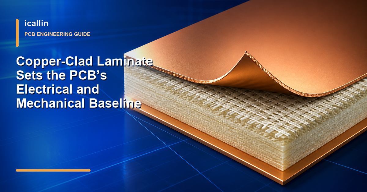
The important word is finished. A multilayer board is a pressed construction of cores, prepreg, copper, plating, and surface coatings. The dimension accepted at receiving may not equal the sum of nominal design values. Pressed dielectric thickness, copper distribution, plating, solder mask, and the fabricator's measurement convention all influence the reported result. The drawing should therefore state the required finished thickness, tolerance, datum, and whether surface coatings are included.
Measure the Board the Assembly Will Receive
Finished thickness is measured from one outer board surface to the other at defined locations. A single measurement near an edge may miss local variation, while a reading over a raised copper feature or heavy solder mask may not represent the laminate body. Card-edge products, press-fit hardware, and sealed enclosures often need a location-specific inspection plan.
The familiar 1.6 mm value is common, but it is not a universal mechanical standard. Connectors may be designed around a different card thickness, and even a connector advertised for a nominal board size has an acceptable range. The board drawing and connector data sheet must agree on the same finished condition. The same check applies to guide rails, bezels, retaining clips, thermal pads, and mounting hardware.
Thin boards can help reduce product height or mass, but they may flex during handling, assembly, or connector insertion. A thicker board is usually stiffer when material, outline, and support conditions remain comparable. That does not make thickness a complete structural specification. Cutouts, copper distribution, component mass, mounting span, temperature, and laminate construction can dominate bending and warpage.
Fit, Stiffness, and Stackup Are Different Decisions
Thickness affects several design domains, but each requires its own evidence.
| Design question | What thickness changes | What must be checked separately |
|---|---|---|
| Connector or enclosure fit | Card section, guide clearance, insertion geometry | Connector acceptance range, finish buildup, tolerance, inspection location |
| Board stiffness | Bending resistance and handling response | Material, outline, support span, cutouts, component mass, warpage |
| Multilayer stackup | Available dielectric spacing and total pressed construction | Impedance model, resin content, copper distribution, plane references, press data |
| Drilling and vias | Finished aspect ratio and possible stub length | Drill diameter, plating, reliability class, backdrill or blind/buried-via plan |
| Power and thermal behavior | Space available for a construction | Copper cross-section, thermal path, airflow, interfaces, temperature rise |
Thickness and signal integrity are linked through the actual stackup, not through a rule that thicker is better. Increasing the overall board dimension can increase dielectric spacing, but the impedance result depends on trace geometry, copper thickness, dielectric constant, reference-plane location, and fabrication tolerances. A thicker board can also lengthen through-hole vias and unused stubs. High-speed behavior must be modeled from the released stackup.

Do Not Use Board Thickness as a Proxy for Copper
A thicker PCB does not automatically carry more current. Trace current capability depends mainly on copper cross-section, allowed temperature rise, routing environment, adjacent copper, and cooling. A thick dielectric beneath a narrow trace does not turn that trace into a high-current conductor.
The same caution applies to heat. More laminate may add mechanical mass, but it does not guarantee a lower component temperature. Heat must travel through copper, thermal vias, planes, interface materials, airflow, a chassis, or a heatsink. Increasing dielectric thickness can even lengthen a poor through-board thermal path. Thermal performance needs a defined path and a temperature model or measurement.
Nor does extra thickness automatically improve voltage safety. Creepage follows surfaces, clearance crosses air, and dielectric withstand depends on the specified insulation system. Those requirements should be calculated and documented independently.
Build the Requirement From the Product Inward
Start with the interfaces that cannot move: connector slot, enclosure opening, mounting stack, keypad height, optical alignment, or heat-spreader position. Convert those limits into a finished board range, not just a nominal target. Include worst-case tolerances from the board, connector, fasteners, and mating parts.
Next, create a stackup that meets that mechanical range while supporting impedance, plane pairing, voltage isolation, copper weight, and via reliability. Ask the selected fabricator to confirm available core and prepreg constructions and the finished-thickness convention before layout release. A proposed substitution in glass style, resin content, or copper weight can move both electrical spacing and final thickness.
The fabrication note should identify:
- nominal finished thickness and permitted tolerance;
- whether solder mask and other coatings are included;
- controlled measurement locations when fit is local;
- released layer stack, copper weights, and impedance requirements;
- card-edge, press-fit, or enclosure dimensions that require inspection;
- any coupon or acceptance method needed for the product.
Prototype measurements are useful only when the test matches production intent. Record the tool, measurement locations, environmental condition when relevant, and observed range. If connector engagement is critical, verify the assembled interface rather than relying on an isolated thickness reading.
Frequently Asked Questions
Does a thicker PCB automatically carry more current?
No. Current capacity is controlled primarily by trace or plane copper cross-section, temperature-rise limits, layout, and cooling. Board thickness can affect the available stackup, but it is not a substitute for copper and thermal design.
Is 1.6 mm the standard thickness for every PCB?
No. It is a widely used nominal value, not a universal requirement. The correct finished thickness comes from connector, enclosure, mechanical, electrical, and fabrication constraints, together with a stated tolerance and inspection method.
Conclusion
Finished PCB thickness is a shared mechanical and stackup requirement. It should be chosen from product fit, stiffness, dielectric construction, and via constraints, then released with a clear tolerance and measurement definition. Keeping copper current, thermal paths, signal integrity, and safety calculations separate prevents a convenient nominal thickness from becoming an unsupported engineering shortcut.
Need Help With PCB Manufacturing or PCBA Assembly?
Share your PCB manufacturing or PCBA assembly requirements with icallin through our dedicated quotation page.